Body-biased pMOS protection against electrostatic discharge

a pmos and body-biased technology, applied in the direction of semiconductor devices, semiconductor/solid-state device details, electrical apparatus, etc., can solve the problems of thermal runaway in the device, severe damage to the integrated circuit,

Active Publication Date: 2007-08-14
TEXAS INSTR INC
View PDF7 Cites 9 Cited by
  • Summary
  • Abstract
  • Description
  • Claims
  • Application Information

AI Technical Summary

Benefits of technology

[0010]It is a technical advantage of the present invention that energy for biasing the substrate of the ESD protection circuit is provided by the ESD pulse. This feature eliminates the need to supply an additional voltage source to the ESD protection circuit.
[0011]It is another technical advantage that the concept of substrate biasing for uniform discharge transistor triggering can be applied to multifinger transistors.
[0012]It is another technical advantage that the protection pMOS transistor can be applied with its gate tied to its source through a series resistor such that CDM protection is built in.
[0013]Since the invention employs a discrete resistor, the bias resistor / network generates robust pumping, and is independent of any n-well (or p-well) process changes or variations. The invention thus applies to a wide family of semiconductor processes and devices.
[0014]Each pMOS transistor finger has the whole length or at least a large fraction in a high conduction state due to the more uniform potential across the n-well, according to the invention. This stands in contrast to conventional technology with its standard nMOS in an unconfined p-well.
[0015]In the invention, the pump current is confined to the n-well and cannot turn on output nMOS transistors, or trigger latch-up in neighboring circuits. Further, the substrate biasing of the ESD protection circuit is provided only during an ESD event. The drawbacks associated with prior substrate biasing schemes are not experienced.

Problems solved by technology

Integrated circuits (ICs) may be severely damaged by electrostatic discharge (ESD) events.
Second breakdown is a phenomenon that induces thermal runaway in the device wherever the reduction of the impact ionization current is offset by the thermal generation of carriers.

Method used


Image

  • Body-biased pMOS protection against electrostatic discharge
  • Body-biased pMOS protection against electrostatic discharge
  • Body-biased pMOS protection against electrostatic discharge

Examples


Embodiment Construction

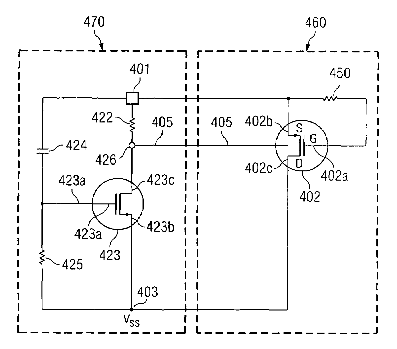
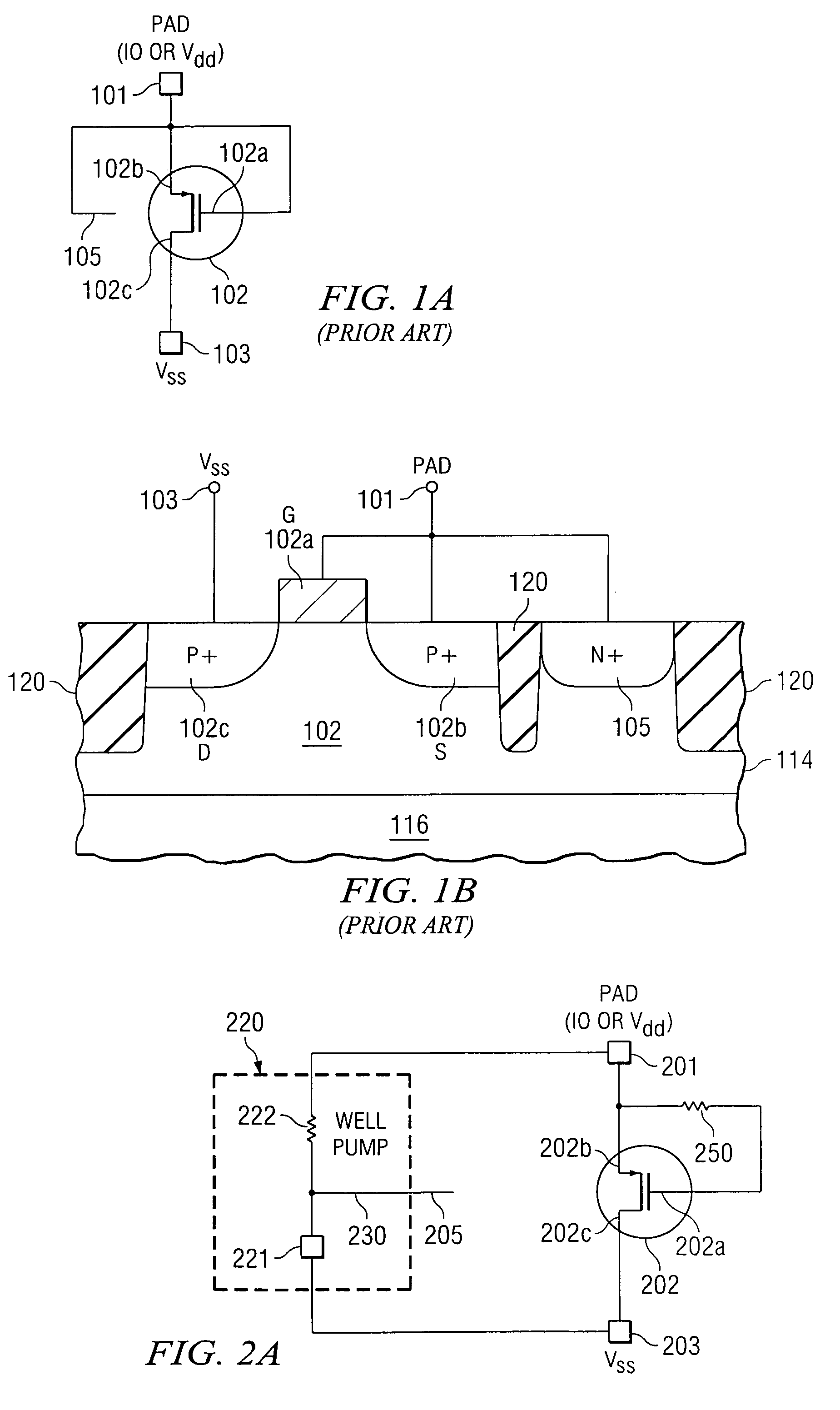
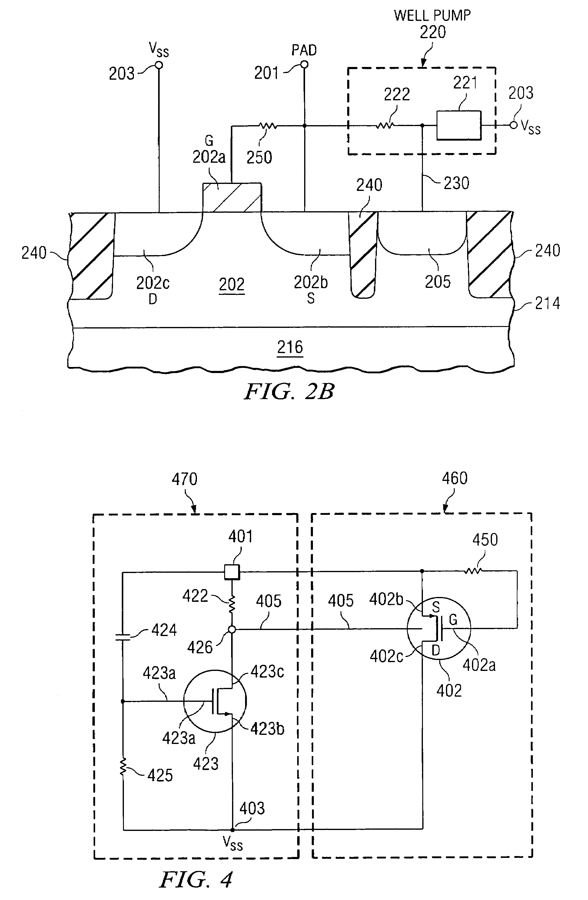
[0029]The present invention is related to U.S. Pat. No. 5,940,258, issued on Aug. 17, 1999 (Duvvury, “Semiconductor ESD Protection Circuit”).

[0030]FIGS. 2A and 2B are a schematic circuit diagram and cross section of an ESD protection circuit, which is included in an integrated circuit (IC) in addition to other devices in the IC. These ICs can typically be found in processors, digital and analog devices, and other high performance devices. ESD protection is an integral part of an IC and is typically used at each input / output pin in order to discharge any electrical transients received at the IC before they enter the IC and cause damage to electrostatic sensitive components.

[0031]In FIGS. 2A and 2B, 201 represents a pad (input / output, power, Vdd). It is fabricated on the semiconductor substrate 202, usually silicon of a first conductivity type. In the preferred embodiment, the first conductivity type is p-type; it should be stressed, however, that all following considerations also hol...


PUM


Abstract

A protection circuit for protecting an integrated circuit pad 201 against an ESD pulse, which comprises a discharge circuit having an elongated MOS transistor 202 (preferably pMOS) in a substrate 205 (preferably n-type), said discharge circuit operable to discharge the ESD pulse to the pad, to ground 203. The embodiment further contains a pump circuit connected to the pad for receiving a portion of the pulse's current; the pump circuit comprises a component 221 determining the size of this current portion (for example, another transistor, a string of forward diodes, or a reverse Zener diode), wherein the component is connected to ground. A discrete resistor 222 (for example about 40 to 60Ω) is connected between the pad and the component and is operable to generate a voltage drop (about 0.5 to 1.0 V) by the current portion. A plurality of contacts to the substrate connects to the resistor so that the voltage drop is uniformly impressed on the substrate to ensure uniform turn-on of the elongated transistor for uniform pulse discharge.

Description

FIELD OF THE INVENTION[0001]The present invention is related in general to the field of electronic systems and semiconductor devices and more specifically to structure and method of electrostatic discharge circuits including uniformly activated pMOS protection devices.DESCRIPTION OF THE RELATED ART[0002]Integrated circuits (ICs) may be severely damaged by electrostatic discharge (ESD) events. A major source of ESD exposure to ICs is from the human body (described by the “Human Body Model”, HBM); the discharge of the human body generates peak currents of several amperes to the IC for about 100 ns. A second source of ESD is from metallic objects (described by the “Machine model”, MM); it can generate transients with significantly higher rise times and current levels than the HBM ESD source. A third source is described by the “charged device model” (CDM), in which the IC itself becomes charged and discharges to ground in rise times less than 500 ps.[0003]ESD phenomena in ICs are growin...

Claims


Application Information

Patent Timeline
Patent Type & Authority Patents(United States)
IPC IPC(8): H01L23/62
CPCH01L27/0277
Inventor SALLING, CRAIG T.DUVVURY, CHARVAKABOSELLI, GIANLUCA
Owner TEXAS INSTR INC
Why Eureka
Try Eureka