Package-integrated thin film LED

Active Publication Date: 2007-08-14
LUMILEDS
View PDF14 Cites 205 Cited by
  • Summary
  • Abstract
  • Description
  • Claims
  • Application Information

AI Technical Summary

Benefits of technology

[0014]The LED layers are extremely thin (less than 50 microns and typically less than 3 microns) so there is very little absorption of light by the thinned GaN layer; there is high thermal conductivity to the package because the LED layers are directly bonded to the package s

Problems solved by technology

The support substrate between the LED layers and the package provides some electrical and thermal resistance, which is undesirable.
The suppo

Method used


Image

  • Package-integrated thin film LED
  • Package-integrated thin film LED
  • Package-integrated thin film LED

Examples


Embodiment Construction

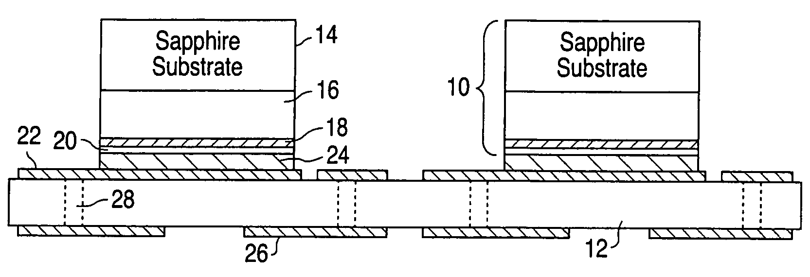
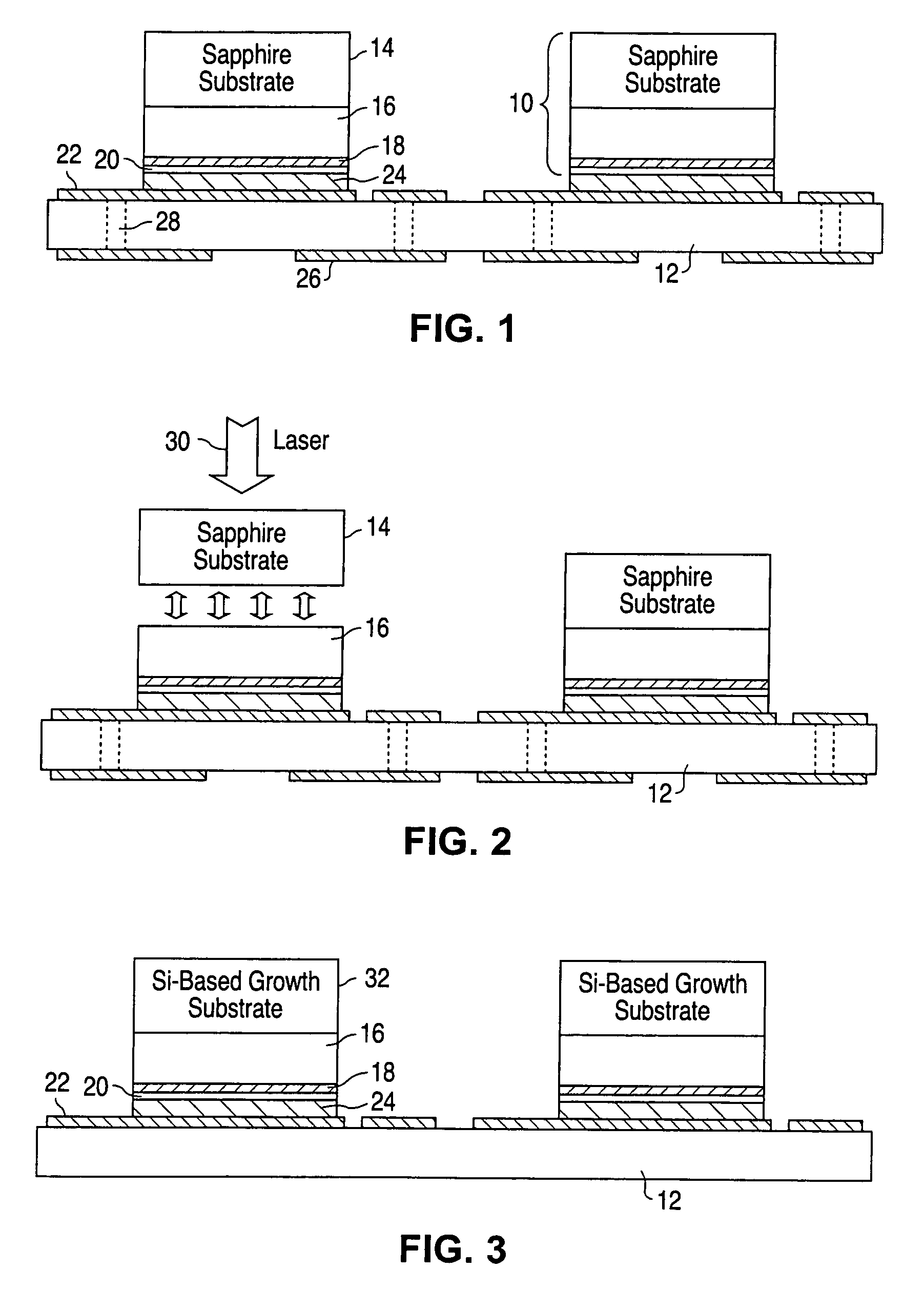
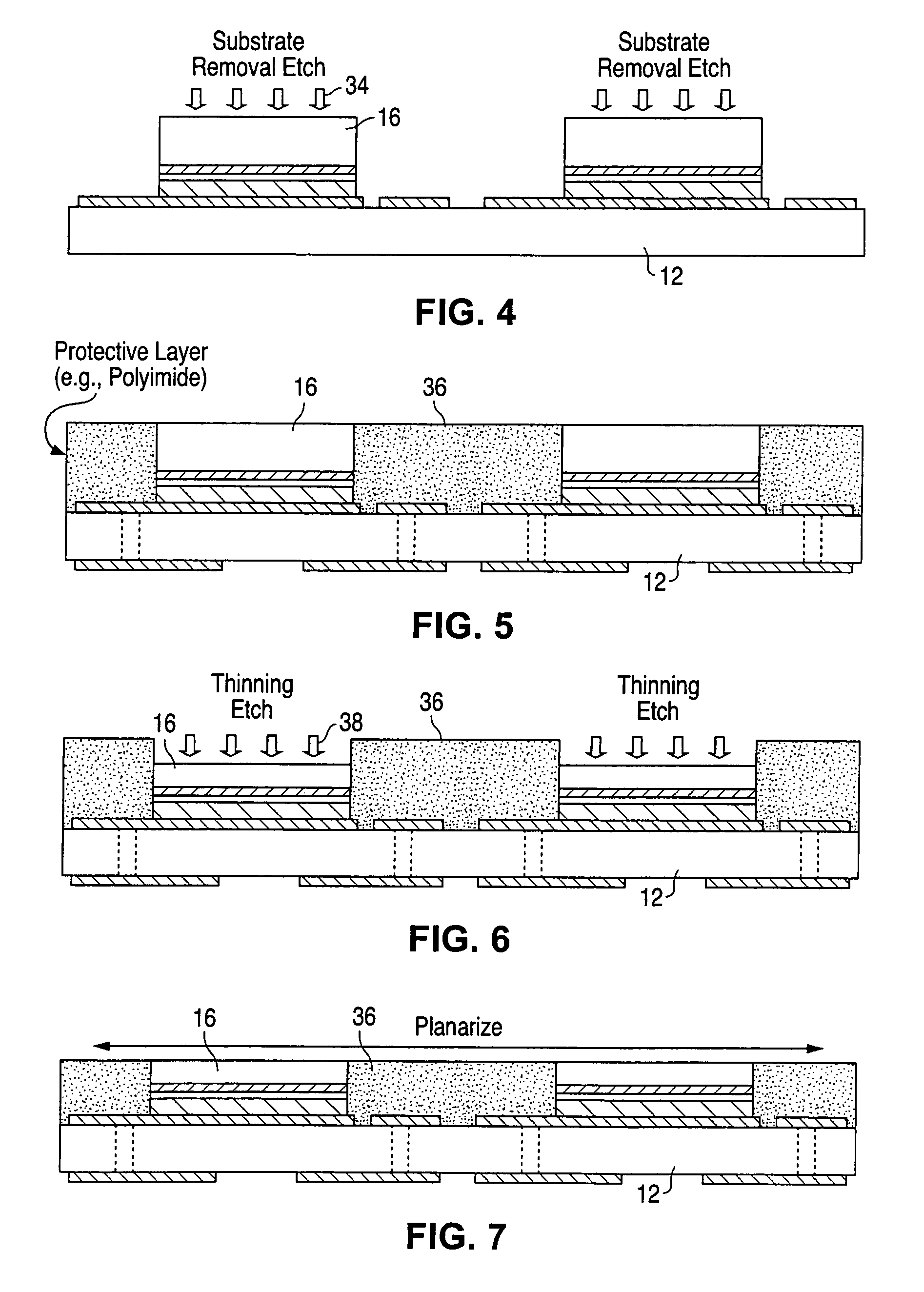
[0035]A process for providing a very thin LED on a package substrate, without any growth substrate or support substrate, is described with respect to FIGS. 1–16.

[0036]As a preliminary matter, a conventional LED is formed on a growth substrate. In the example used, the LED is a GaN-based LED, such as an AlInGaN LED. The term GaN will be used to represent any GaN-based material. Typically, a relatively thick (approx. 1–2 micron) undoped or n-type GaN layer is grown on a sapphire growth substrate using conventional techniques. Other substrates may also be used, such as SiC, Si, SiCOI, and ZnO. In the case of gallium-phosphide (III-P) LEDs, the growth substrate is typically GaAs or Ge. The relatively thick GaN layer typically includes a low temperature nucleation layer and one or more additional layers so as to provide a low-defect lattice structure for the n-type cladding layer and active layer.

[0037]One or more n-type cladding layers are then formed over the thick n-type layer, follow...


PUM


Abstract

LED epitaxial layers (n-type, p-type, and active layers) are grown on a substrate. For each die, the n and p layers are electrically bonded to a package substrate that extends beyond the boundaries of the LED die such that the LED layers are between the package substrate and the growth substrate. The package substrate provides electrical contacts and conductors leading to solderable package connections. The growth substrate is then removed. Because the delicate LED layers were bonded to the package substrate while attached to the growth substrate, no intermediate support substrate for the LED layers is needed. The relatively thick LED epitaxial layer that was adjacent the removed growth substrate is then thinned and its top surface processed to incorporate light extraction features. There is very little absorption of light by the thinned epitaxial layer, there is high thermal conductivity to the package because the LED layers are directly bonded to the package substrate without any support substrate therebetween, and there is little electrical resistance between the package and the LED layers so efficiency (light output vs. power input) is high. The light extraction features of the LED layer further improves efficiency.

Description

FIELD OF THE INVENTION[0001]This invention relates to light emitting diodes (LEDs) and, in particular, to a technique for mounting LED dies for packaging so the packaged LEDs have improved optical, electrical, and thermal characteristics.BACKGROUND[0002]LEDs are formed by growing epitaxial layers, including p-type and n-type layers, on a growth substrate. A light-emitting active layer is sandwiched between the n and p layers. Green, blue, and ultraviolet LEDs are typically gallium-nitride based, where the growth substrate is typically either sapphire (an insulator), SiC (a semiconductor), silicon, SiC-on-insulator (SiCOI), or other engineered substrate. Infrared, red, and amber LEDs are typically some combination of AlInGaPAs and grown on a GaAs or InP substrate. The growth substrate has a lattice structure similar to the lattice structure of the LED material.[0003]It is sometimes desirable to remove the growth substrate to, for example, improve the optical properties of the LED or ...

Claims


Application Information

Patent Timeline
IPC IPC(8): H01L23/495H01L33/00H01L33/48
CPCH01L33/0079H01L33/486H01L33/32H01L33/48H01L33/22H01L2224/32225H01L2224/48091H01L2224/48227H01L2224/73265H01L2924/00014H01L2224/48464H01L2224/92247H01L2924/00012H01L2924/00H01L24/73H01L2224/45014H01L33/0093H01L2924/206
Inventor EPLER, JOHNMARTIN, PAUL S.KRAMES, MICHAEL R.
Owner LUMILEDS
Why Eureka
Try Eureka