Thin-film deposition apparatus

a technology of thin film and deposition apparatus, which is applied in the direction of mechanical equipment, vacuum evaporation coating, coating, etc., can solve the problems of reducing throughput, difficult to control the thickness of thin film at the molecular layer level, and generating particles, and achieves a reduction of the purge time of residual gas

Active Publication Date: 2007-09-11
ASM JAPAN
View PDF11 Cites 15 Cited by
  • Summary
  • Abstract
  • Description
  • Claims
  • Application Information

AI Technical Summary

Benefits of technology

[0010]Consequently, an object of the present invention in an embodiment is to provide a thin-film deposition apparatus enabling considerable reduction of the purge time of residual gas by completely separating the reaction area and the transfer area.

Problems solved by technology

If the residual gas remains inside the reactor, CVD reaction occurs in the vapor phase, making it difficult to control film thickness at the molecular layer level.
Additionally, it causes a problem of generation of particles because a particle size generated becomes larger during vapor phase reaction.
To completely evacuate residual gas from within the reactor, conventionally a prolonged purge process was required; as a result, throughput was declined.
This method, however, was not able to completely prevent reaction gas from entering into the transfer area by diffusion; unwanted films deposited by CVD reaction were observed inside the transfer area.
This indicates that the transfer area is at risk of particle generation because residual reaction gas cannot be completely evacuated except expediting a maintenance cycle.
Additionally, it is difficult to shorten the purge time as well by this method.
Because more processes use higher-frequency RF power as the wafer diameter has increased in recent years, impedance of a heater itself, which is embedded inside the susceptor, cannot be ignored in such processes.
These accumulates can exfoliate and cause particle contamination.

Method used


Image

  • Thin-film deposition apparatus
  • Thin-film deposition apparatus
  • Thin-film deposition apparatus

Examples


Embodiment Construction

[0044]The invention will be explained further with reference to specific embodiments, but the invention should not be limited thereto.

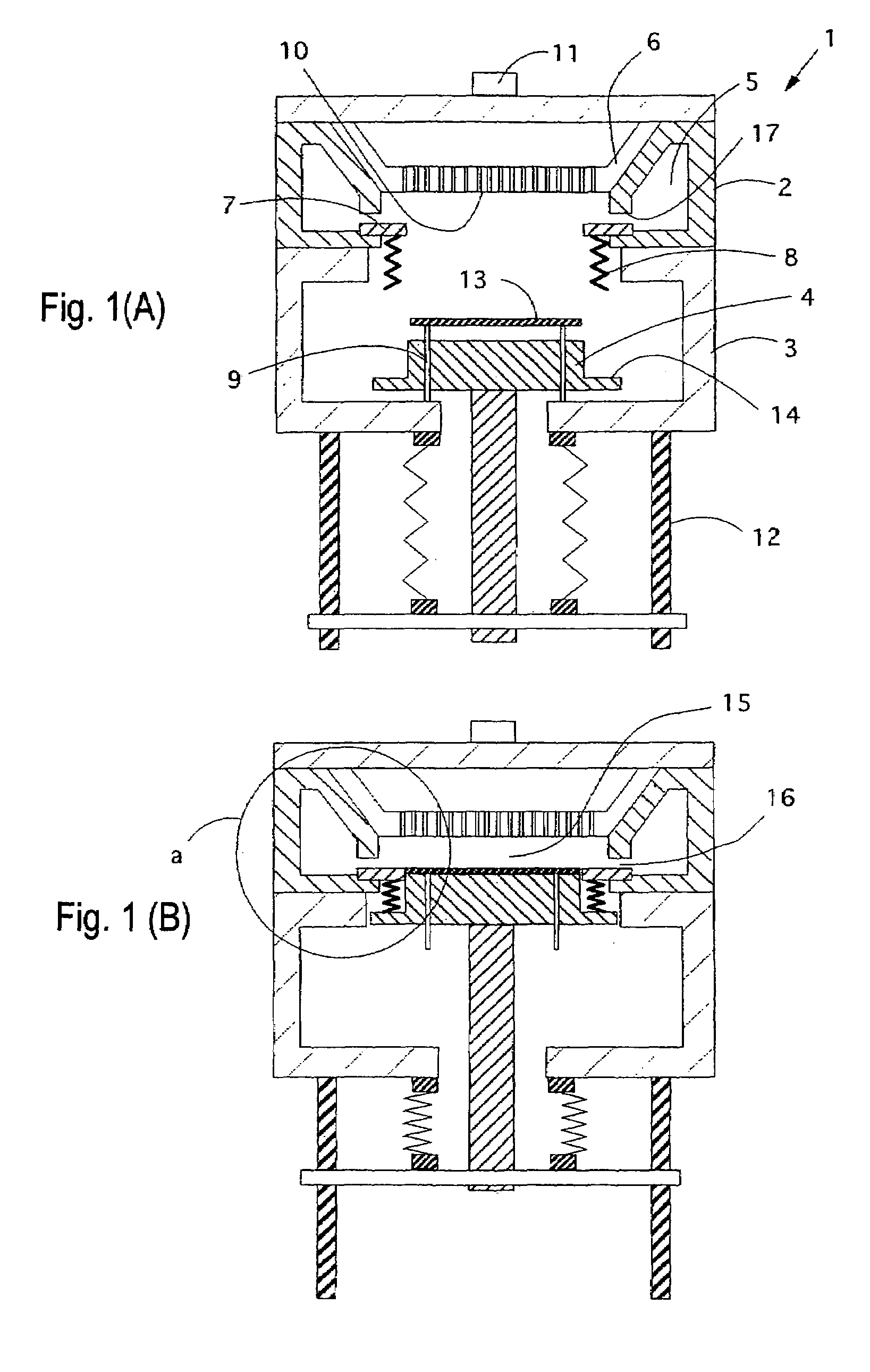
[0045]The present invention is described in detail with reference to figures. FIGS. 1(A) and 2(B) show cross-sectional schematic views of a preferred embodiment for carrying out the thin-film deposition apparatus according to the present invention. FIG. 1(A) shows a position, in which a semiconductor substrate is carried into a substrate transfer chamber from a load-lock chamber (not shown). FIG. 1(B) shows a position in which deposition reaction takes place.

[0046]A thin-film deposition apparatus 1 according to an embodiment of the present invention comprises the reaction chamber 2 and the substrate transfer chamber 3. Inside the thin-film deposition apparatus 1, a susceptor 4 for placing a semiconductor substrate 13 on it is provided. The susceptor 4 moves up and down between the reaction chamber 2 and the substrate transfer chamber 3 by an elevating...


PUM

PropertyMeasurementUnit
temperatureaaaaaaaaaa

Abstract

A thin-film deposition apparatus includes a reaction chamber, a substrate transfer chamber, a susceptor having a radially-extending step portion, a ring-shaped separation wall for separating the reaction chamber and the substrate transfer chamber at a processing position where the susceptor is positioned inside the ring-shaped separation wall, and a conductive sealing member which is interposed between the radially-extending step portion and the separation wall to seal the reaction chamber from the substrate transfer chamber when the susceptor is at a processing position.

Description

BACKGROUND OF THE INVENTION[0001]1. Field of the Invention[0002]The present invention relates to a thin-film deposition apparatus which forms a thin film on a semiconductor substrate, and, in particular, to a thin-film deposition apparatus which allows complete separation of a reaction chamber and a substrate transfer chamber.[0003]2. Description of the Related Art[0004]As semiconductor apparatuses have become highly integrated, ALCVD (Atomic Layer Chemical Vapor Deposition) having high thin-film deposition controllability attracts attention and replaces conventionally-used CVD (Chemical Vapor Deposition). Because ALCVD forms a thin film predominantly by absorption of atoms or molecules onto a semiconductor wafer, which is caused using multiple reaction gases to be absorbed onto the semiconductor wafer, thin-film deposition can deposit one atomic or molecular layer at a time and can form a film being several-molecules thick, and the step coverage of a resultant film is excellent.[00...

Claims


Application Information

Patent Timeline
Patent Type & Authority Patents(United States)
IPC IPC(8): C23C16/00C23F1/00H01L21/306C23C16/44C23C16/455C23C16/458C23C16/54F16J3/04F16J15/08H01L21/205
CPCC23C16/4401C23C16/45544C23C16/4585C23C16/54F16J3/047F16J15/0887
Inventor KAWANO, BAIEI
Owner ASM JAPAN
Why Eureka
Try Eureka