

Emissive display using organic electroluminescent devices
- Summary
- Abstract
- Description
- Claims
- Application Information
AI Technical Summary
Benefits of technology
Problems solved by technology
Method used
Image

Examples
first embodiment
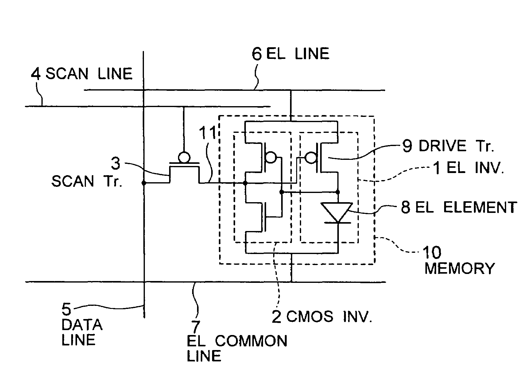
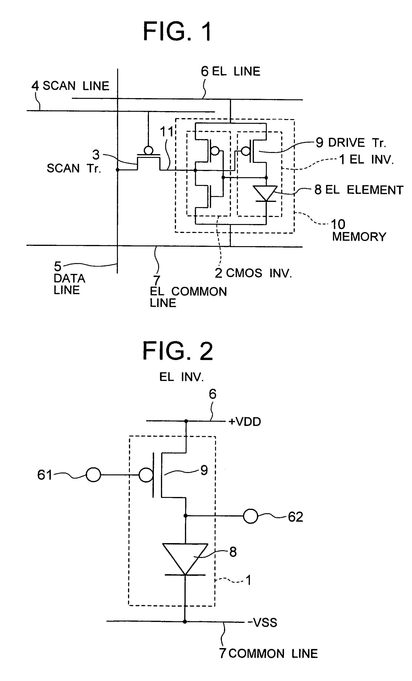
[0032]Hereinafter, a plurality of embodiments of the present invention will be explained in detail by using the accompanying drawings. FIG. 1 shows a pixel circuit configuration of a display which is a In the pixel, a scan line 4 and a data line 5 are arranged so that they intersect with each other, and a region enclosed by the lines is a pixel region. Furthermore, an EL power supply line 6, and an EL common line 7 are connected.
[0033]In the inside of the pixel, a memory circuit 10 including an EL inverter circuit 1 comprised of an EL device 8 and a driving transistor 9, and including a CMOS inverter circuit 2 formed by CMOS connection is arranged. The memory circuit 10 is connected to the data line 5 through a main circuit of a scan transistor 3, and a gate of the scan transistor 3 is connected to the scan line 4.
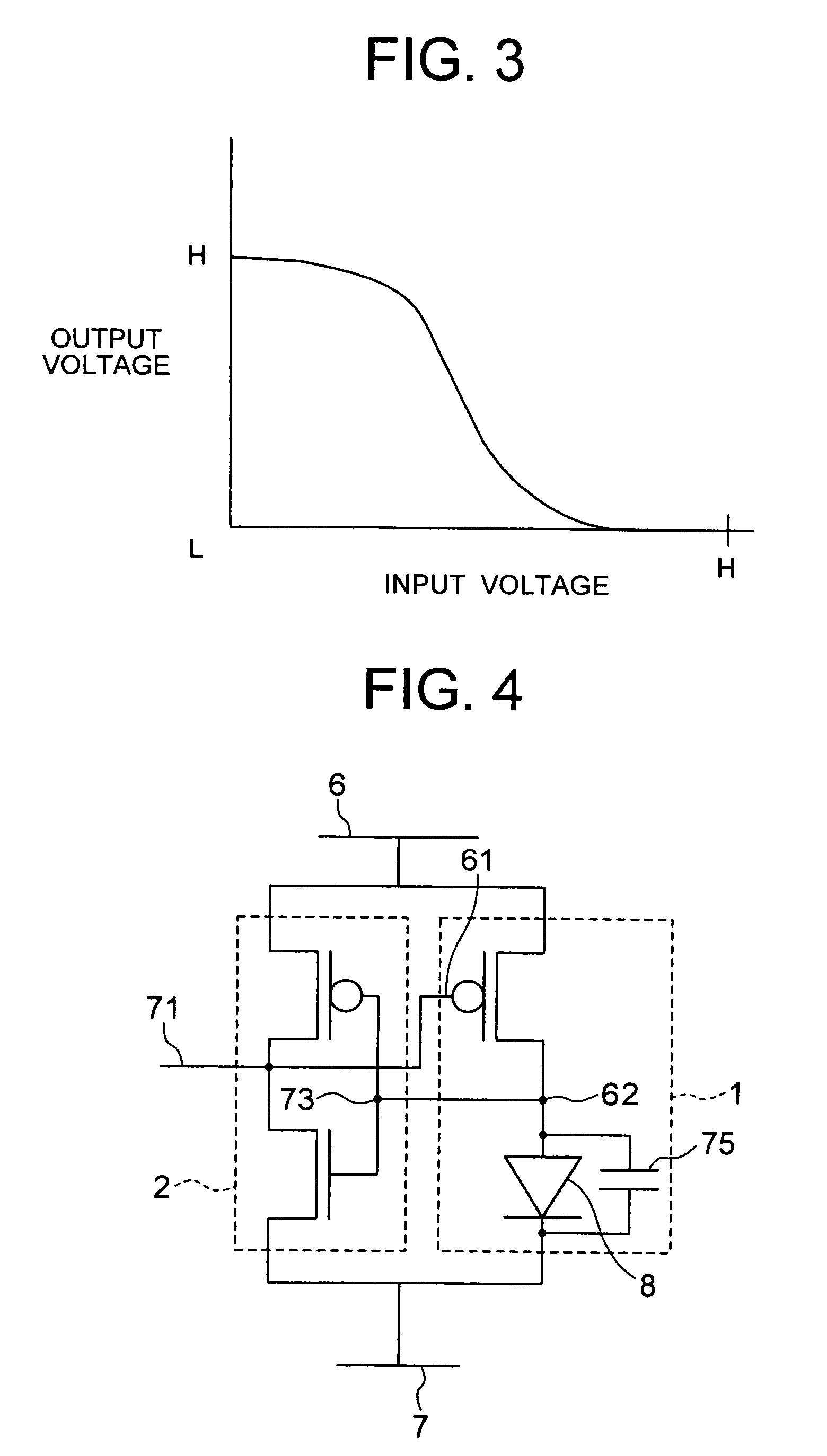
[0034]FIG. 2 shows the operation of the EL inverter circuit 1. The driving transistor 9 is a p-channel transistor, and its source terminal is connected to the EL power su...
second embodiment
[0048]Next, a second embodiment shown in FIG. 7 will be explained. In the present embodiment, the transistors within the pixel are all formed by only p-channel type having the same threshold value characteristic. By this configuration, the feature is that the transistor fabrication process is simplified, and it is possible to manufacture at low cost.
[0049]In the circuit configuration, the EL device 8 and the driving transistor 9 have the same configuration as the first embodiment. The other set of inverter is not the CMOS inverter, but a PMOS inverter 47 in which all the transistors are formed by p-channel transistors. The operation of this circuit will be explained below.
[0050]The PMOS inverter 47 is formed by two p-channel transistors including a reset transistor 46 and a set transistor 43, and one MOS diode which is a bias diode 44, and a bias capacitance 45. The set transistor 43 is turned on when it changes the output of inverter 47 to a L-(logical low) level. In order to chang...
third embodiment
[0055]Furthermore, as a circuit configuration for small power consumption, there is a third embodiment in which all the transistors are formed by n-channel type transistors. As shown in FIG. 8, all the transistors are formed by N-type. They are a scan transistor 143, set transistor 142, reset transistor 144, and bias diode 145.
[0056]The circuit operation is the same as the second embodiment. When it is intended to form this circuit with thin-film transistors, since it is possible to reduce the current during off state of the transistors to a great extent by employing the leakage current reducing structure such as a LDD structure with N-ch TFT, and a series connection configuration of transistors, the power consumption of circuit can be further reduced as compared with the second embodiment. As to the configuration for reducing the leakage current, a general method may be used.
[0057]In the second and third embodiments, when the on state of pixel is continued, both the set transistor ...
PUM
 Abstract
Description
Claims
Application Information