Industrial microdeposition system for polymer light emitting diode displays, printed circuit boards and the like

a light-emitting diode display and micro-deposition technology, applied in the field of micro-deposition systems, can solve the problems of contaminating both the substrate and the fluid material, high production quantity to amortize the cost of fabrication equipment, and relatively expensive implementation of manufacturing techniques, etc., and achieve the effect of increasing the resolution of features

Inactive Publication Date: 2007-09-18
ULVAC INC
View PDF12 Cites 54 Cited by
  • Summary
  • Abstract
  • Description
  • Claims
  • Application Information

AI Technical Summary

Benefits of technology

[0013]In still other features, a head assembly provides a mounting surface for the head. The head positioning module adjusts pitch by rotating the head assembly. The controller generates an over-clocking signal that is used to improve feature resolution. The nozzle firing module adjusts timing of the nozzle firing commands using the over-clocking signal to compensate for changes to the pitch.
[0020]In other features, a laser is mounted on one of the head assembly and a laser head assembly, the laser is used to increase feature resolution.

Problems solved by technology

Most of these manufacturing techniques are relatively expensive to implement and require high production quantities to amortize the cost of the fabrication equipment.
Contact also occurs between the screen and the fluid material, which contaminates both the substrate and the fluid material.
Therefore, screen printing is not a viable option for the manufacture of certain microstructures.
One obstacle to the widespread use of PLED display devices is the difficulty encountered to manufacture PLED display devices.
Photolithography is also not compatible with PLED display devices Manufacturing processes using photolithography generally involve the deposition of a photoresist material onto a substrate.
However, photolithography contaminates the substrate and the material formed on the substrate.
Photolithography is not compatible with the manufacture of PLED displays because the photoresist contaminates the PLED polymers.
The cost of the photolithography process can be prohibitive when relatively small quantities are to be fabricated.
Spin coating is also an expensive process because a majority of the fluid material does not remain on the substrate.
In addition, the size of the substrate is limited by the spin coating process to less than approximately 12″, which makes spin coating unsuitable for larger devices such as PLED televisions.

Method used


Image

  • Industrial microdeposition system for polymer light emitting diode displays, printed circuit boards and the like
  • Industrial microdeposition system for polymer light emitting diode displays, printed circuit boards and the like
  • Industrial microdeposition system for polymer light emitting diode displays, printed circuit boards and the like

Examples


Embodiment Construction

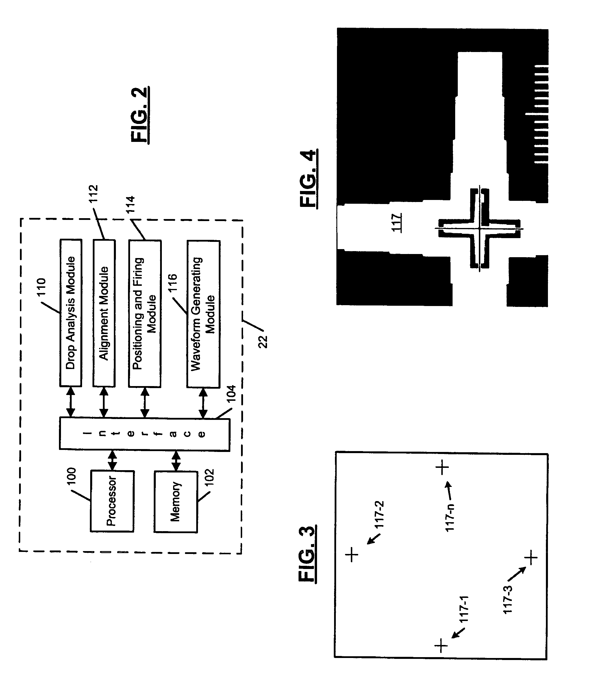
[0061]The following description of the preferred embodiment(s) is merely exemplary in nature and is in no way intended to limit the invention, its application, or uses. For purposes of clarity, the same reference numbers will be used in the drawings to identify similar elements.

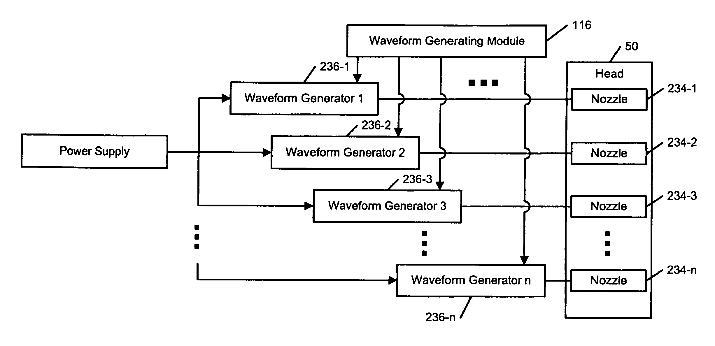
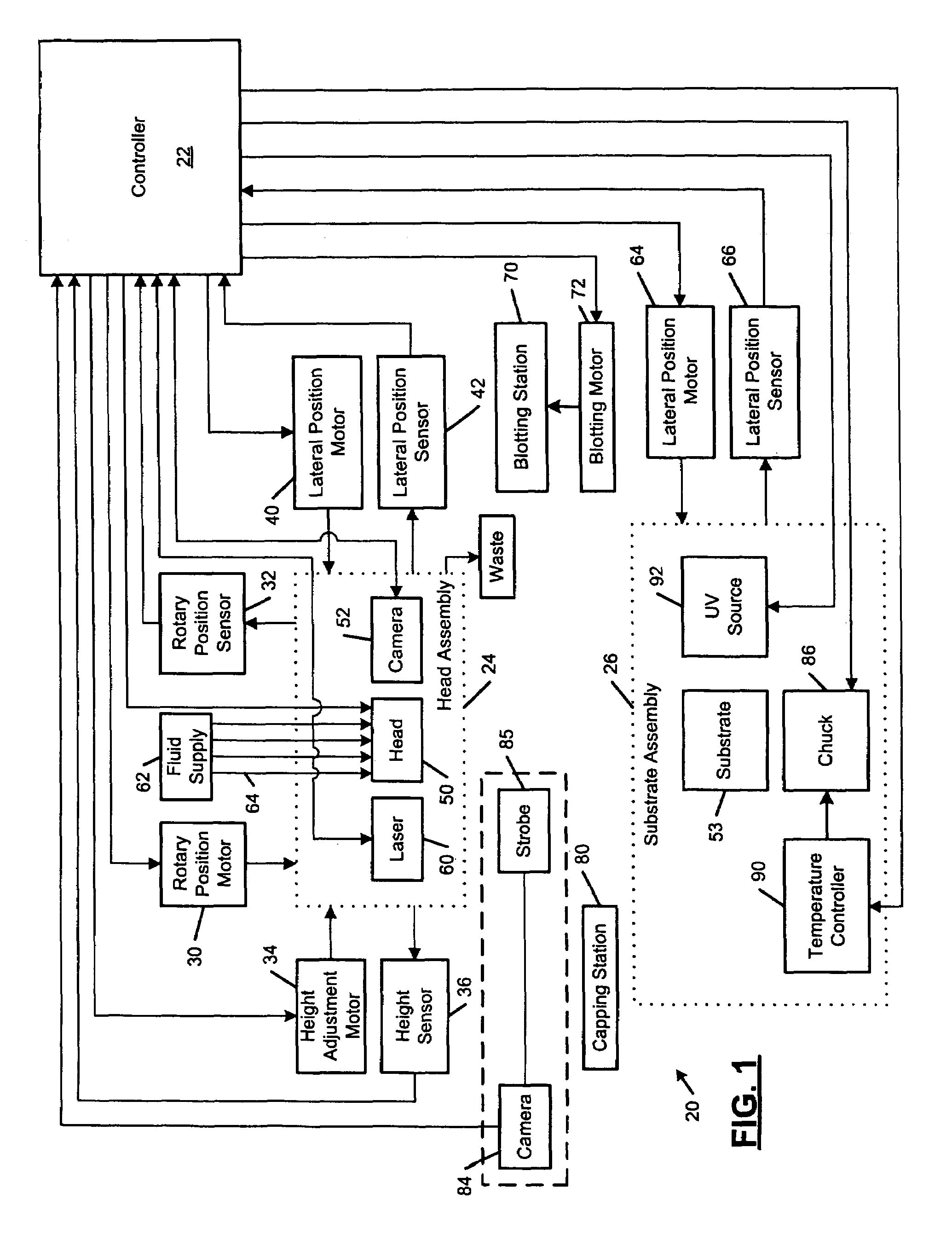
[0062]Referring now to FIG. 1, a microdeposition system 20 is illustrated and includes a controller 22, a head assembly 24, and a substrate assembly 26. A rotational position or pitch of the head assembly 24 is adjusted using a rotary position motor 30 and a rotary position sensor 32. Likewise, a height of the head assembly 24 relative to the substrate assembly 26 may be adjusted using a height adjustment motor 34 and a height sensor 36. A lateral position of the head assembly 24 is adjusted using a lateral position motor 40 and a lateral position sensor 42.

[0063]According to the invention, an ink jet head can deposit fluid manufacturing materials in manufacturing environments to form any of a wide variety of...


PUM

PropertyMeasurementUnit
thicknessesaaaaaaaaaa
temperatureaaaaaaaaaa
distanceaaaaaaaaaa

Abstract

A microdeposition system (20) and method deposits precise amounts of fluid material onto a substrate. A microdeposition head (50) includes a plurality of spaced nozzles. A positioning device controls a position of the microdeposition head relative to the substrate. A controller (22) includes a positioning module that communicates with the positioning device and that generates position control signals for the positioning device. A nozzle firing module communicates with the microdeposition head (50) and selectively generates nozzle firing commands to define features of at least one layer of an electrical device, such as resistors, traces and capacitors on a printed circuit board, polymer light emitting diodes, and light panels.

Description

CROSS-REFERENCE TO RELATED APPLICATIONS[0001]This application is a 371 of PCT / US02 / 17523 which was filed on May 31, 2002, and which claims the benefit of U.S. Provisional Patent Application Ser. No. 60 / 295,118, entitled “Formation of Microstructures Using Piezo Deposition of Liquid Onto Substrate,” filed Jun. 1, 2001, and U.S. Provisional Application Ser. No. 60 / 295,100, entitled Formation Of Printed Circuit Board Structures Using Piezo Deposition Of Liquid Onto Substrate, filed Jun. 1, 2001, each of which is incorporated herein by reference.FIELD OF THE INVENTION[0002]The present invention relates to microdeposition systems, and more particularly to microdeposition systems for fabricating printed circuit boards, polymer light emitting diode (PLED) displays, and other devices requiring microdeposition of fluid material.BACKGROUND OF THE INVENTION[0003]Manufacturers have developed various techniques for fabricating microstructures that have small feature sizes on substrates. Typicall...

Claims


Application Information

Patent Timeline
Patent Type & Authority Patents(United States)
IPC IPC(8): B05C11/10B05C5/00B05D1/26B05C9/12B05C9/14B05C11/00B05D3/00B25B11/00B29C67/00B41J2/01B41J2/04B41J2/045B41J2/05B41J2/055B41J3/407B41J3/54H01L21/00H01L21/683H01L23/12H01L51/50H05B33/10H05K1/02H05K3/06H05K3/12H05K13/04
CPCB25B11/005B29C67/0059B41J2/04B41J2/04505B41J2/04506B41J2/0451B41J2/04558B41J2/0456B41J2/04573B41J2/04575B41J2/04581B41J2/04588B41J2/0459B41J2/04591B41J2/04593B41J2/04596B41J3/407B41J3/543H01L21/67103H01L21/6715H01L21/67248H01L21/6838H05K3/125B41J2202/04B41J2202/09H05K1/0269H05K3/0008H05K2201/09918B29C64/112B29C64/188H01L21/20
Inventor EDWARDS, CHARLES O.ALBERTALLI, DAVIDBIELICH, HOWARD WALTERMIDDLETON, JAMESBRUNER, SCOTT R.
Owner ULVAC INC
Why Eureka
Try Eureka