Manufacturing method of thin film integrated circuit device and manufacturing method of non-contact type thin film integrated circuit device

a manufacturing method and technology of integrated circuits, applied in semiconductor devices, semiconductor/solid-state device details, instruments, etc., can solve the problems of limiting the design range, increasing manufacturing costs, and reducing the yield of substrates, so as to achieve effective use of substrates, reduce manufacturing costs, and improve yield and throughput.

Inactive Publication Date: 2007-09-18
SEMICON ENERGY LAB CO LTD
View PDF56 Cites 151 Cited by
  • Summary
  • Abstract
  • Description
  • Claims
  • Application Information

AI Technical Summary

Benefits of technology

[0009]However, with non-contact type and contact type IC chips becoming common, it is necessary to mass-produce enormous amount of IC chips, which are utilizable for human beings, animals and plants, commercial products, banknotes, and the like, at the lowest cost. For example, it is necessary to manufacture IC chips to be applied to commercial products, banknotes, and the like at a cost of 1 to several yen per IC chip, preferably, at a cost less than 1 yen, and it is desired to realize a structure and a manufacturing process of an IC chip that can be mass-produced at low cost.

Problems solved by technology

However, since the silicon wafer is all polished and removed in spite of its expensive price, the increase in manufacturing cost is unavoidable.
Further, since the integrated circuit using the silicon wafer is thick, depressions and projections are produced in a surface to limit the range of choice for designing in the case of mounting into a product container.
However, this method has a possibility that the substrate is not completely separated due to a factor such as stress distribution of a thin film formed on the substrate.

Method used


Image

  • Manufacturing method of thin film integrated circuit device and manufacturing method of non-contact type thin film integrated circuit device
  • Manufacturing method of thin film integrated circuit device and manufacturing method of non-contact type thin film integrated circuit device
  • Manufacturing method of thin film integrated circuit device and manufacturing method of non-contact type thin film integrated circuit device

Examples


embodiment mode 1

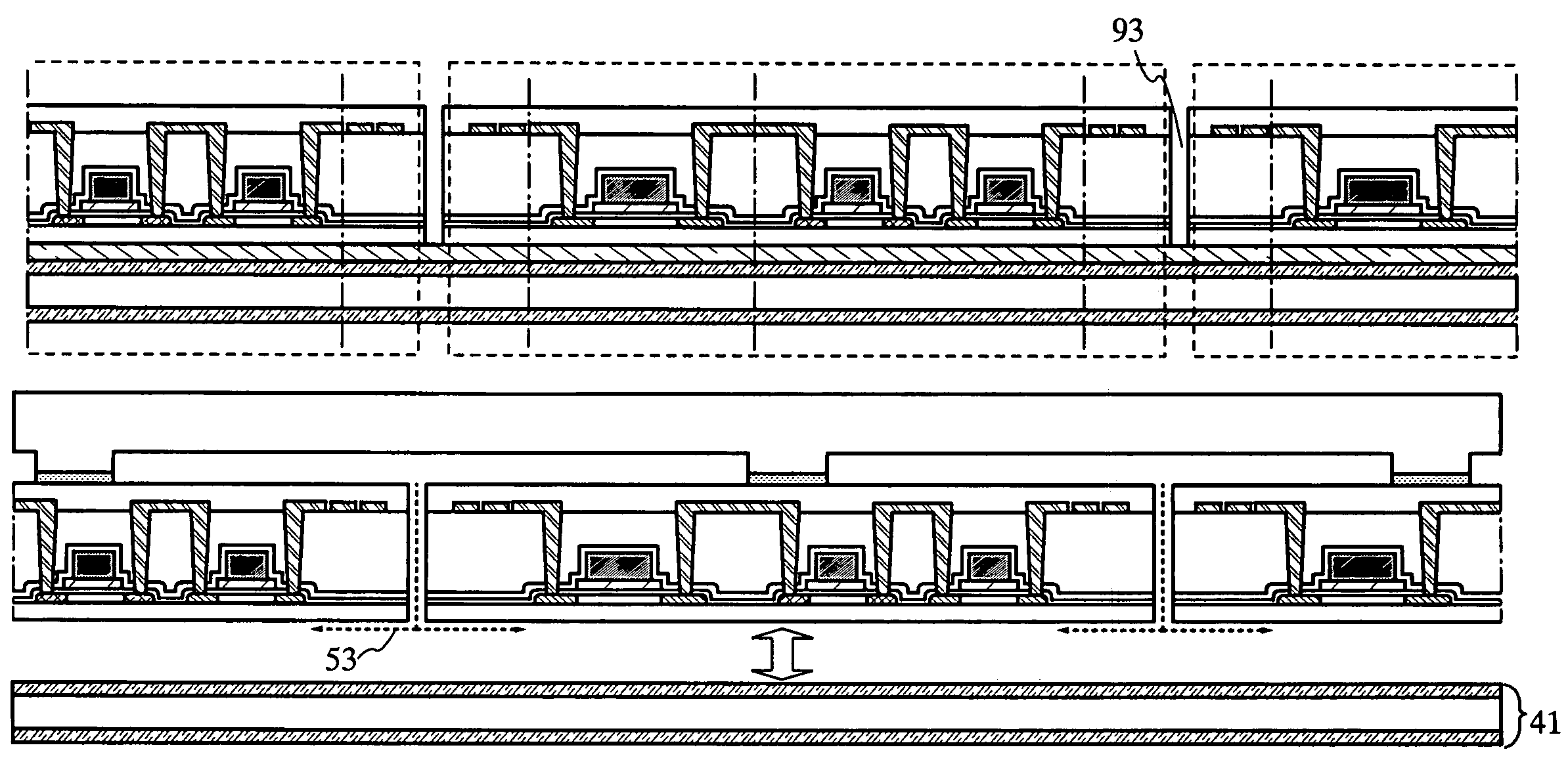
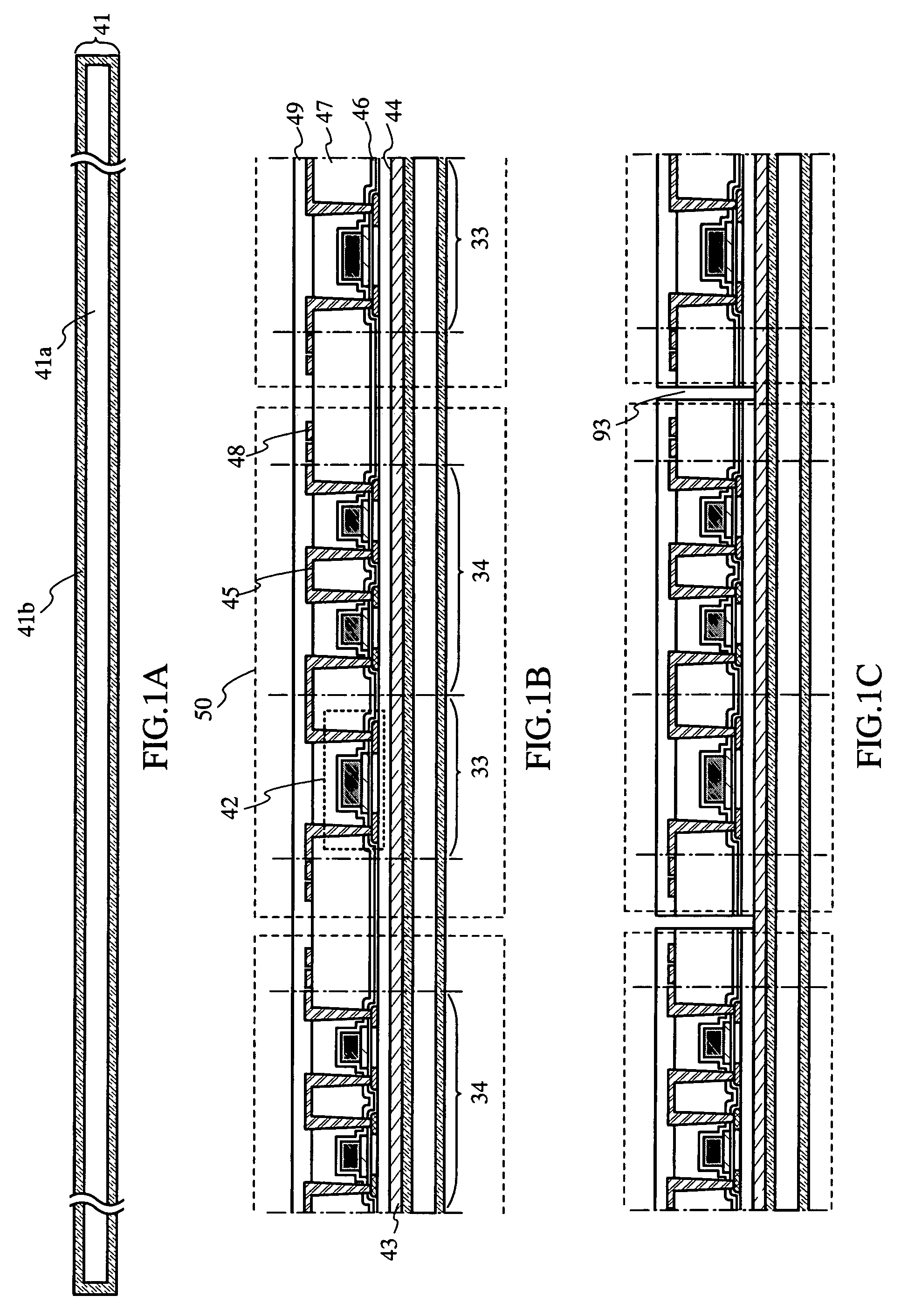
[0085]A thin film integrated circuit device and manufacturing method thereof according to the present invention will be described with reference to mainly FIGS. 1A to 1C, FIGS. 2A to 2C, and FIGS. 3A and 3B. First, a silicon wafer 41a is prepared, and an oxide film 41b (silicon oxide film) is formed at a surface of the silicon wafer 41a by performing a thermal treatment to obtain a thermally oxidized silicon substrate 41 (FIG. 1A). As a method for the thermal treatment, a thermal treatment at 800 to 1200° C. (preferably at about 900° C. or 1150° C.) may be performed, which, however, is not limited to these temperatures.

[0086]Although all surfaces or at least one surface of the semiconductor substrate may be oxidized, it is preferable that all of the surfaces are oxidized to form silicon oxide, in order not to damage the semiconductor substrate when halogen fluoride such as ClF3 is used to separate a thin film integrated circuit device from the substrate later. This is because silico...

embodiment mode 2

[0108]In the present embodiment mode, a case of using dry etching for forming the groove 93 will be described with reference to FIGS. 4A to 4C. FIG. 4A is the same as Embodiment Mode 1 up to the state of FIG. 1A. Thereafter, a resist 54 is formed over the substrate by processes of exposure and development, and a groove 93 is formed by dry etching with the resist 54 as a mask to separate devices (FIG. 4A). Plasma etching is employed here, and a chlorine-based gas typified by Cl2, BCl3, SiCl4, CCl4, or the like, a fluorine-based gas typified by CF4, SF6, NF3, or CHF3, or the like or O2 is used as an etching gas, which is not limited to these. The etching can be performed by utilizing atmospheric pressure plasma. In this case, it is preferable to use a mixed gas of CF4 and O2 as an etching gas. Alternatively, etching with the use of a different kind of gas may be performed several times to form the groove 93.

[0109]After the etching, the resist 54 is left as it is, and made to function ...

embodiment mode 3

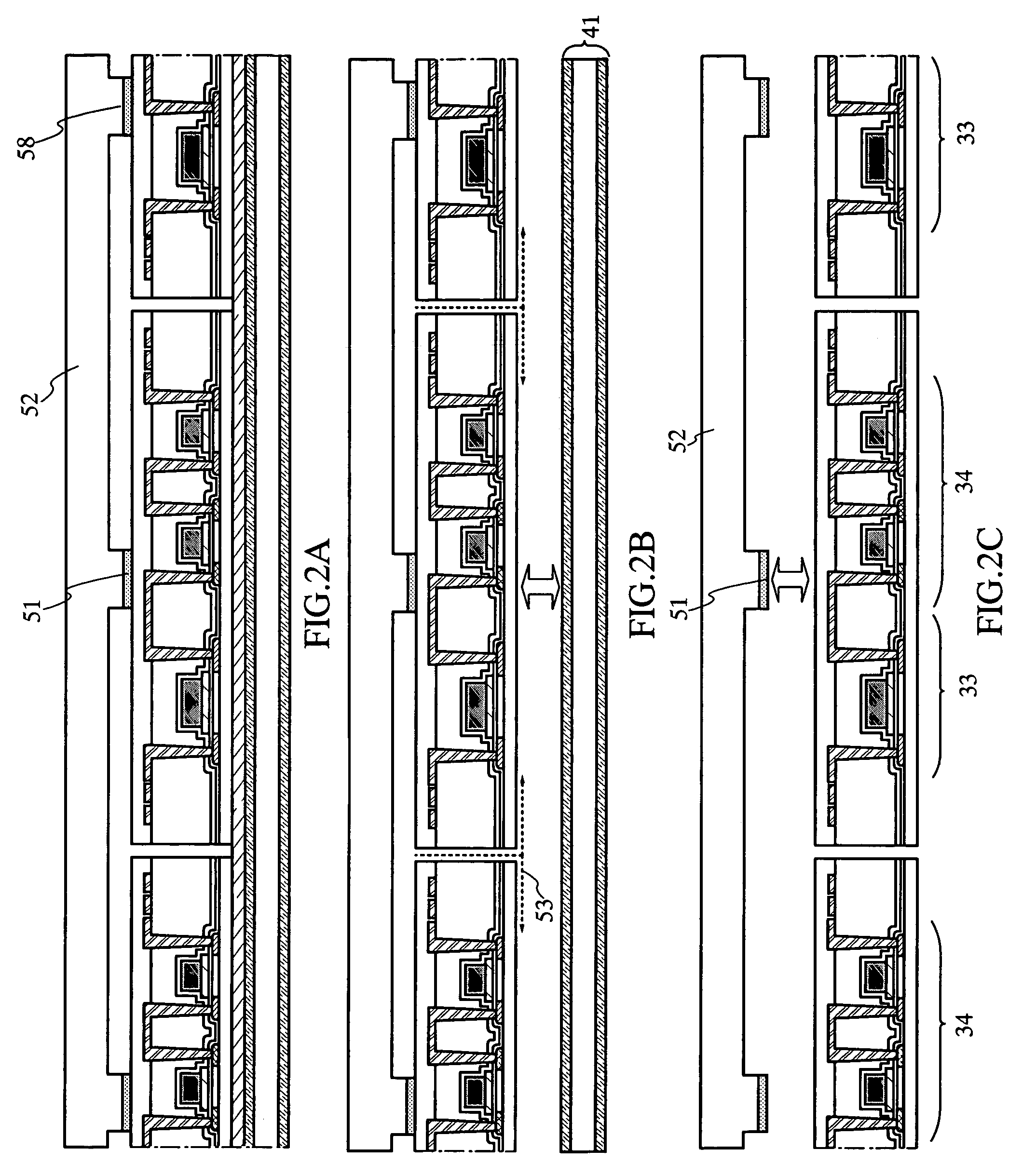
[0112]In the present embodiment mode, a case will be described, where the thermally oxidized silicon substrate 41 or a SOI substrate such as a SIMOX substrate is used again in the case of scratching the substrate on forming the groove 93 by a method such as dicing. As a first method, a planarization film 57 is formed on a used substrate 56 as shown in FIG. 5A. As the planarization film 57, polyimide, acrylic, polyamide, or a heat-resistant resin such as siloxane can be formed by a method such as spin coating, dipping, spraying, or droplet discharge (for example, inkjet). In consideration of thermal treatment of a post-process, it is preferable to use a heat-resistant resin such as siloxane. Alternatively, an inorganic material such as PSG (phosphosilicate glass), BPSG (borophosohposilicate glass), or alumina may be used. The following processes are the same as in Embodiment Mode 1 or 2.

[0113]As a second method, there is a method of using CMP (chemical mechanical polishing) for plana...


PUM


Abstract

A method of manufacturing a thin film integrated circuit device according to the present invention includes steps of forming a peel-off layer over a thermally oxidized silicon substrate, forming a plurality of thin film integrated circuit devices over the peel-off layer with a base film interposed therebetween, forming a groove between the plurality of thin film integrated circuit devices, and separating the plurality of thin film integrated circuit devices by introducing one of a gas and a liquid including halogen fluoride into the groove to remove the peel-off layer.

Description

BACKGROUND OF THE INVENTION[0001]1. Field of the Invention[0002]The present invention relates to a method of manufacturing a thin film integrated circuit device carrying a thin film integrated circuit that has an element such as a memory and a microprocessor (CPU: Central Processing Unit) and is thin and flexible like paper, and to a non-contact type thin film integrated circuit device including the thin film integrated circuit and an antenna, which is used mainly for a card, a tag, a label, or the like for identifying human beings, animals and plants, commercial products, banknotes, and the like.[0003]2. Description of the Related Art[0004]Recently, in all kinds of industrial worlds such as food industry and manufacturing industry, calls have been heightened for strengthening safety and management systems of commercial products, and therewith, the amount of information on the commercial products are increasing. However, the current information on a commercial product is just inform...

Claims


Application Information

Patent Timeline
Patent Type & Authority Patents(United States)
IPC IPC(8): H01L21/46H01L21/30H01L21/762G06K19/07G06K19/077H01L21/00H01L21/68H01L21/82H01L23/02H01L23/498H01L27/00
CPCG06K19/0704G06K19/0723G06K19/07703G06K19/07718G06K19/07745G06K19/07749G06K19/0775G06K19/07758G06K19/07779G06K19/07781G06K19/07783H01L21/6835H01L23/49855H01L2924/00014H01L2924/01047H01L2924/01015H01L2224/49171H01L2924/10253H01L2224/45147H01L2924/3011H01L2924/30105H01L2924/19041H01L2221/68318H01L2221/68359H01L2221/68368H01L2924/12044H01L2924/00H01L2224/48H01L2924/00011
Inventor YAMAZAKI, SHUNPEITAKAYAMA, TORUKANNO, YOHEI
Owner SEMICON ENERGY LAB CO LTD
Why Eureka
Try Eureka