Methods for forming high density, conformal, silica nanolaminate films via pulsed deposition layer in structures of confined geometry

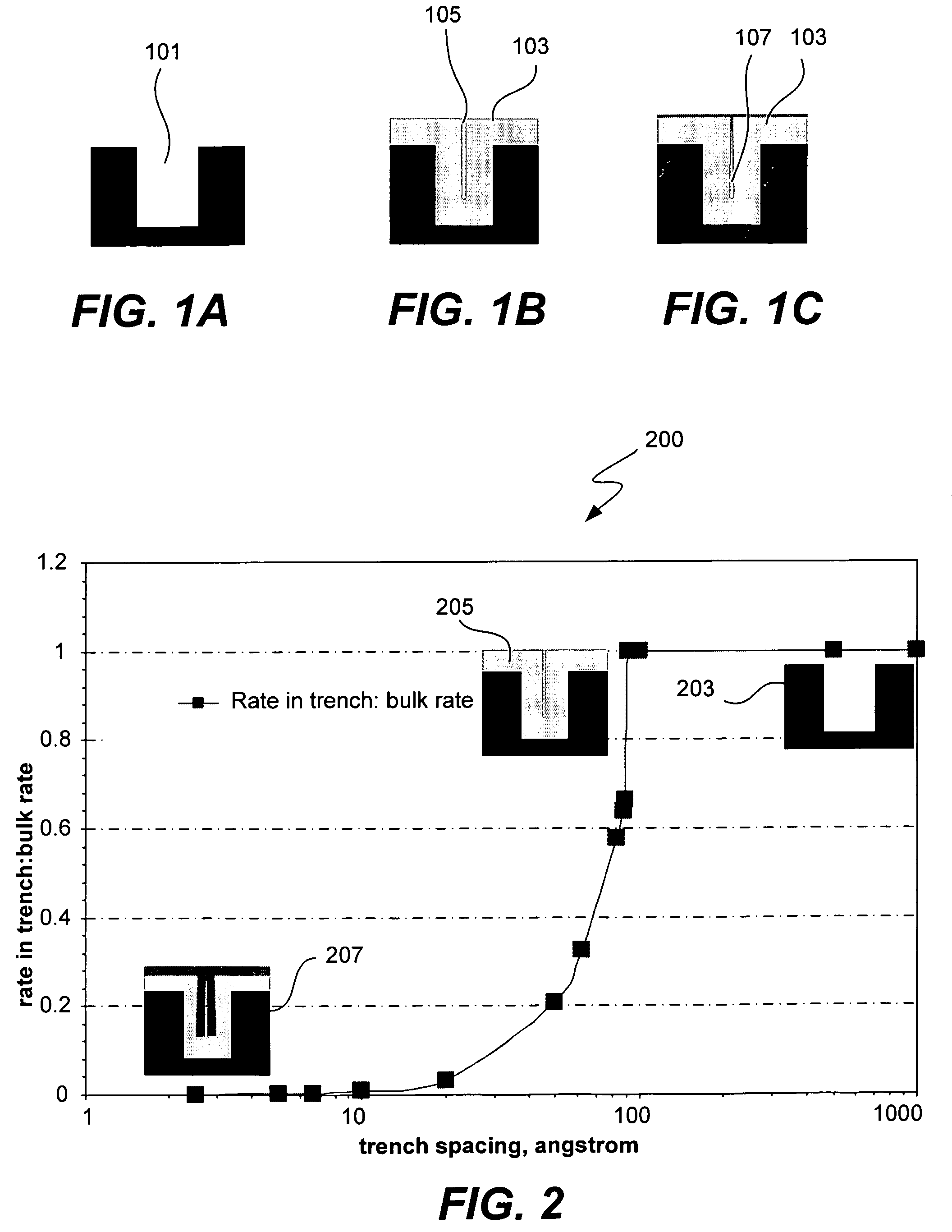
a technology of conformal and silica nanolaminate, which is applied in the direction of chemical vapor deposition coating, coating, metallic material coating process, etc., can solve the problem that the traditional cvd technique cannot provide adequate conformal films in these high aspect ratio features, and the area of low density forming in the film is increased, so as to improve the gap filling in semiconductor device manufacturing, increase density, and eliminate seams and voids

Active Publication Date: 2007-09-18
NOVELLUS SYSTEMS
View PDF52 Cites 21 Cited by
  • Summary
  • Abstract
  • Description
  • Claims
  • Application Information

AI Technical Summary

Benefits of technology

[0008]The present invention meets these needs by providing methods of forming conformal films with increased density. The methods may be used to improve gap fill in semiconductor device manufacturing by eliminating seams and voids. Operating at high reactant partial pressure increases the density o

Problems solved by technology

However, as design rules continue to shrink, the aspect ratios (depth to width) of features increase, and traditional CVD techniques can no longer provide adequately conformal films in these high aspect ratio features.
While ALD and PDL are useful to form conformal films, conventional ALD and PDL processe

Method used


Image

  • Methods for forming high density, conformal, silica nanolaminate films via pulsed deposition layer in structures of confined geometry
  • Methods for forming high density, conformal, silica nanolaminate films via pulsed deposition layer in structures of confined geometry
  • Methods for forming high density, conformal, silica nanolaminate films via pulsed deposition layer in structures of confined geometry

Examples


examples

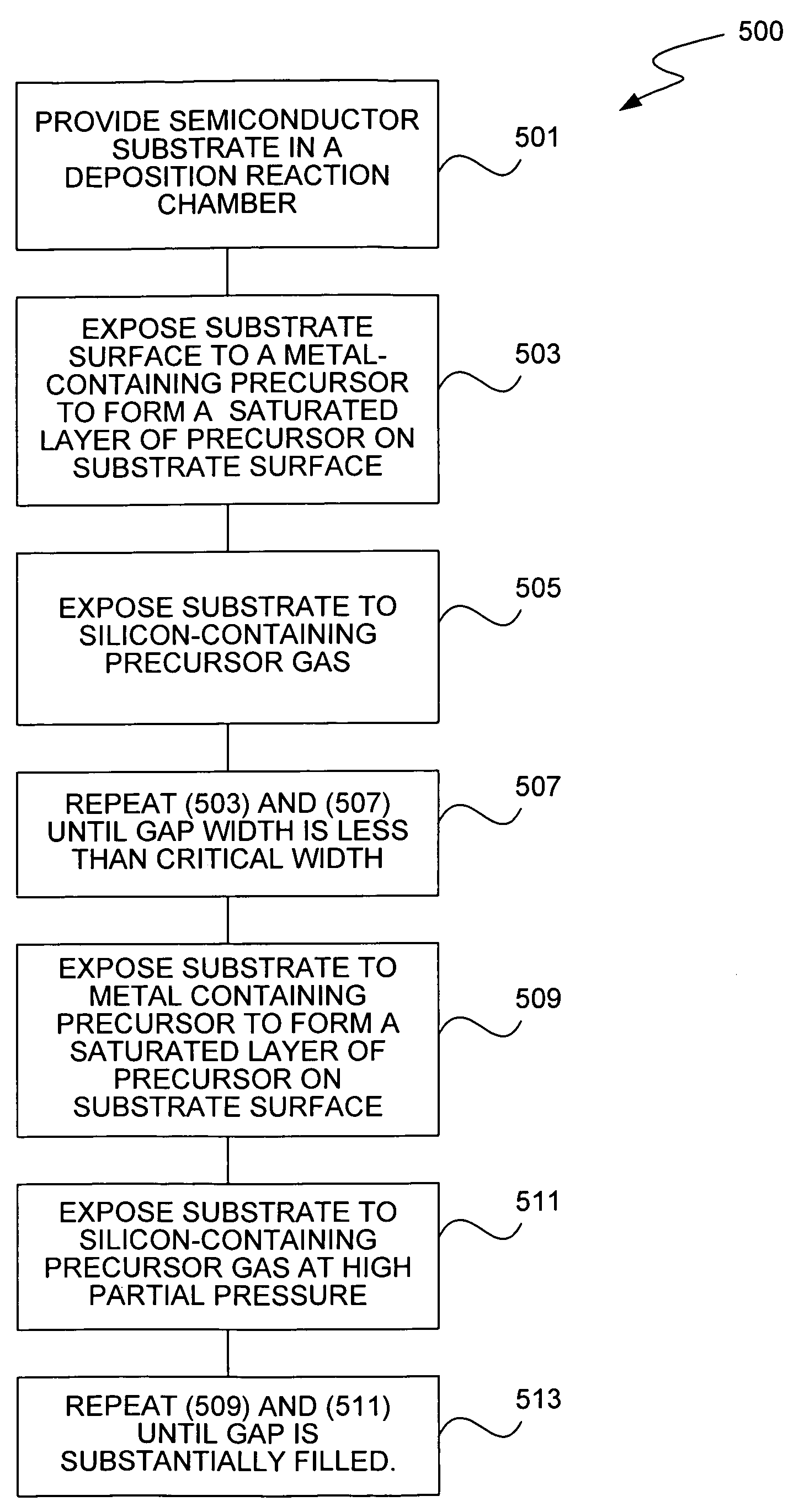
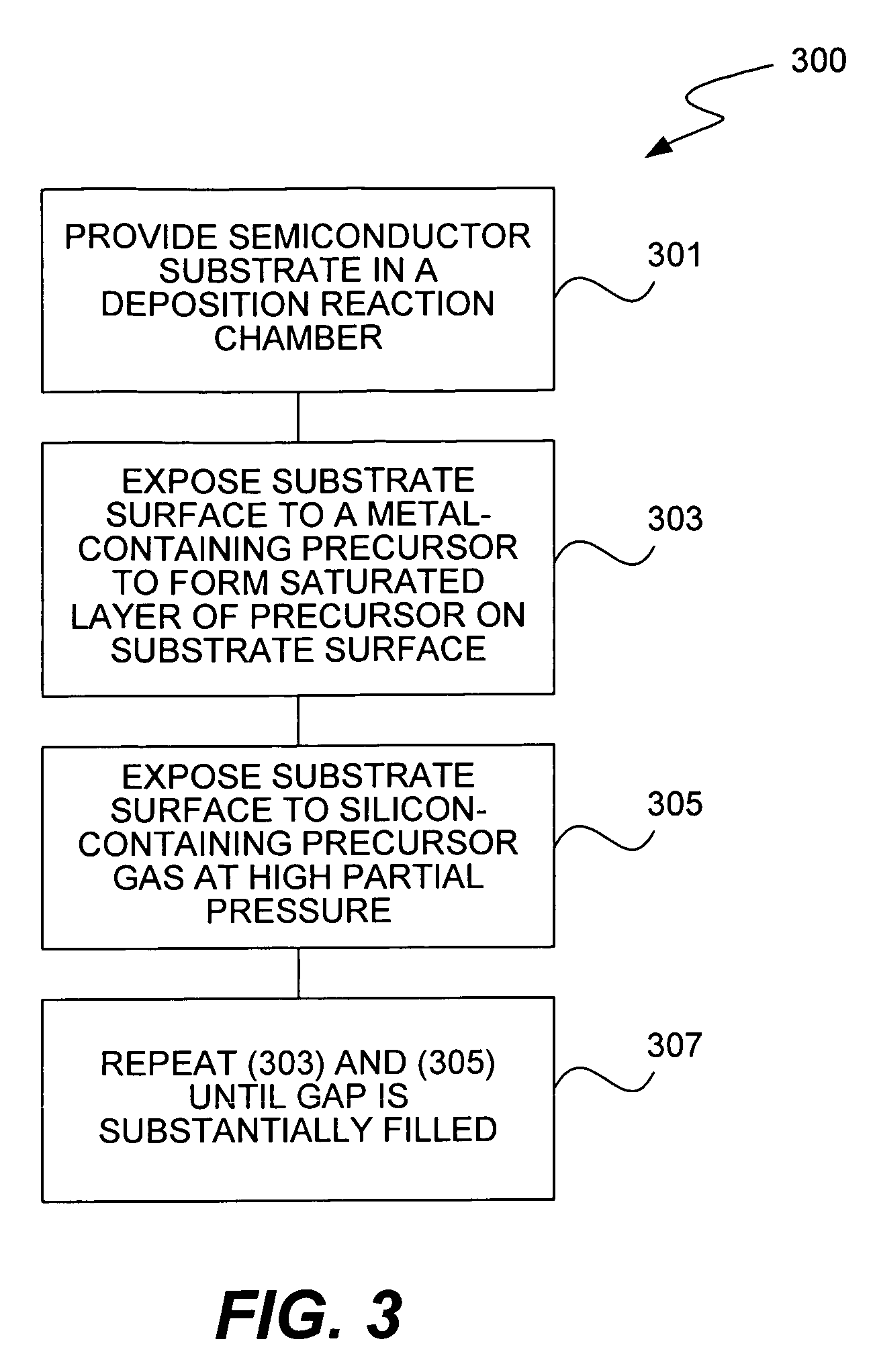
[0050]The following examples provide details illustrating aspects of the present invention. These examples are provided to exemplify and more clearly illustrate these aspects of the invention and are in no way intended to be limiting.

[0051]PDL was employed to fill a trench on a semiconductor substrate. Trimethylaluminum (TMA) was employed as the metal-containing precursor gas. Tris(tert-pentoxy)silanol (TPOSL) was employed as the silicon-containing precursor gas. The substrate was exposed to TPOSL at a partial pressure of 10 Torr. Substrate temperature was 230° C. throughout the process. The process resulted in seam and void-free gap fill as similar to that shown in FIG. 4B.

[0052]The process was repeated for TPOSL partial pressures of 20 Torr and 40 Torr with similar results.


PUM

PropertyMeasurementUnit
Temperatureaaaaaaaaaa

Abstract

Methods of forming conformal films with increased density are described. The methods may be used to improve gap fill in semiconductor device manufacturing by eliminating seams and voids. The methods involve operating at high reactant partial pressure. Additionally, film properties may be further enhanced by optimizing the temperature of the substrate during exposure to the metal-containing and/or silicon-containing precursor gases commonly used in conformal film deposition techniques such as ALD and PDL.

Description

FIELD OF THE INVENTION[0001]This invention pertains to methods for forming high density, conformal, silica nanolaminate films. More specifically, the invention pertains to methods of depositing a conformal film of dielectric material in structures of confined geometry such as high aspect ratio gaps.BACKGROUND OF THE INVENTION[0002]Layers of dielectric film are used in several applications in sub-micron integrated circuits (ICs) fabrication. Four such applications are shallow trench isolation (STI), premetal dielectric (PMD), inter-metal dielectric (IMD) and interlayer dielectric (ILD). All four of these layers require silicon dioxide films that fill features of various sizes and have uniform film thicknesses across the wafer.[0003]Chemical vapor deposition (CVD) has traditionally been the method of choice for depositing conformal silicon dioxide films. However, as design rules continue to shrink, the aspect ratios (depth to width) of features increase, and traditional CVD techniques...

Claims


Application Information

Patent Timeline
IPC IPC(8): H01L21/31
CPCC23C16/045C23C16/45525C23C16/45529H01L21/02145H01L21/02164H01L21/02214H01L21/0228H01L21/3141H01L21/31612
Inventor PAPASOULIOTIS, GEORGE D.TARAFDAR, RAIHAN M.TIPTON, ADRIANNE K.RULKENS, RONHAUSMANN, DENNIS M.TOBIN, JEFF
Owner NOVELLUS SYSTEMS
Why Eureka
Try Eureka