Variable density and variable persistent organic memory devices, methods, and fabrication

a memory device and variable density technology, applied in thermoelectric devices, solid-state devices, instruments, etc., can solve the problems of volatile memory devices losing information, slowing down the speed of other types of storage devices, and increasing the volume, use and complexity of computers and electronic devices, etc., to achieve the ability to store information short term and/or, and improve the efficiency of storag

Active Publication Date: 2007-09-25
MONTEREY RES LLC
View PDF16 Cites 11 Cited by
  • Summary
  • Abstract
  • Description
  • Claims
  • Application Information

AI Technical Summary

Benefits of technology

[0010]The present invention provides semiconductor devices that possess one or more of the following: small size compared to inorganic semiconductor devices, capability to store information short term and / or long term, quick operational response time, lower operating voltages, low cost, high reliability, long life, increased current flow over inorganic semiconductor devices, low temperature processing, light weight, and high density.
[0011]One aspect of the present invention relates to an organic memory device with selectively conductive decay media. This allows variability of the density and variability of the persistence of stored data by altering a resistive state of the organic memory device. Thus, a single device can be utilized, at will, as a long term information storage device with a smaller variable density range and / or as a short term information storage device with a larger variable density range. The same device can be operated in a mixed mode that can be comprised of a plurality of cells having long term storage capability with a small density range; a plurality of cells having a medium term storage capability with a medium density range; and / or a plurality of cells having short, medium, and large density ranges. This eliminates the need for multiple types of storage devices (e.g., volatile and nonvolatile), simplifying memory circuitry, and increasing information storage persistence flexibility on a cell by cell basis.
[0012]In another aspect in accordance with the present invention, a graphical technique varies an amount of memory density versus a retention time of a resulting memory cell. It is to be appreciated varying a memory density versus retention time is a natural extension of a measured response of a utilized memory material. In one aspect in accordance with the present invention, a voltage is applied to a memory cell providing varying densities, wherein the varying density provides an increase or decrease in retention time. Based at least in part upon a measured response curve for a memory material, resistive states are available to a memory cell, wherein an applied voltage changes resistance. The resistance change allows a memory cell to operate in a resistive state, wherein the resistive state is associated with a retention time. A memory cell having more resistive states correlates to a limited retention time. Conversely, a memory cell having limited resistive states correlates to a substantial retention time.
[0013]Another aspect of the present invention relates to a method of fabricating an organic semiconductor device utilizing selectively conductive decay media. This allows formation of an organic memory device that can alter its density and persistence of stored information based upon a resistive state. Fabricating the organic semiconductor device according to the present invention, produces a highly flexible device that can replace multiple devices while decreasing power and area requirements, thus, reducing manufacturing costs and increasing device density.

Problems solved by technology

The volume, use and complexity of computers and electronic devices are continually increasing.
The long term storage mediums typically store larger amounts of information at a lower cost, but are slower than other types of storage devices.
Volatile memory devices generally lose their information if they lose power and typically require periodic refresh cycles to maintain their information.
However, silicon-based devices are approaching their fundamental physical size limits.
Inorganic solid state devices are generally encumbered with a complex architecture which leads to high cost and a loss of data storage density.
The volatile semiconductor memories based on inorganic semiconductor material must constantly be supplied with electric current with a resulting heating and high electric power consumption in order to maintain stored information.
Non-volatile semiconductor devices have a reduced data rate and relatively high power consumption and large degree of complexity.
Currently, devices that can store large amounts of data in a nonvolatile manner, such as hard drives and optical media, are also physically large.
Inorganic type solid state semiconductor devices generally require intricate architectures that directly drive production costs up and data storage density down.
The nonvolatile variety of these semiconductor devices consumes a relatively high amount of power to change states.
And, the volatile variety of these semiconductor devices requires a constant voltage source that consumes even more power than the nonvolatile type.

Method used


Image

  • Variable density and variable persistent organic memory devices, methods, and fabrication
  • Variable density and variable persistent organic memory devices, methods, and fabrication
  • Variable density and variable persistent organic memory devices, methods, and fabrication

Examples


Embodiment Construction

[0034]The following is a detailed description of the present invention made in conjunction with the attached figures, wherein like reference numerals will refer to like elements throughout.

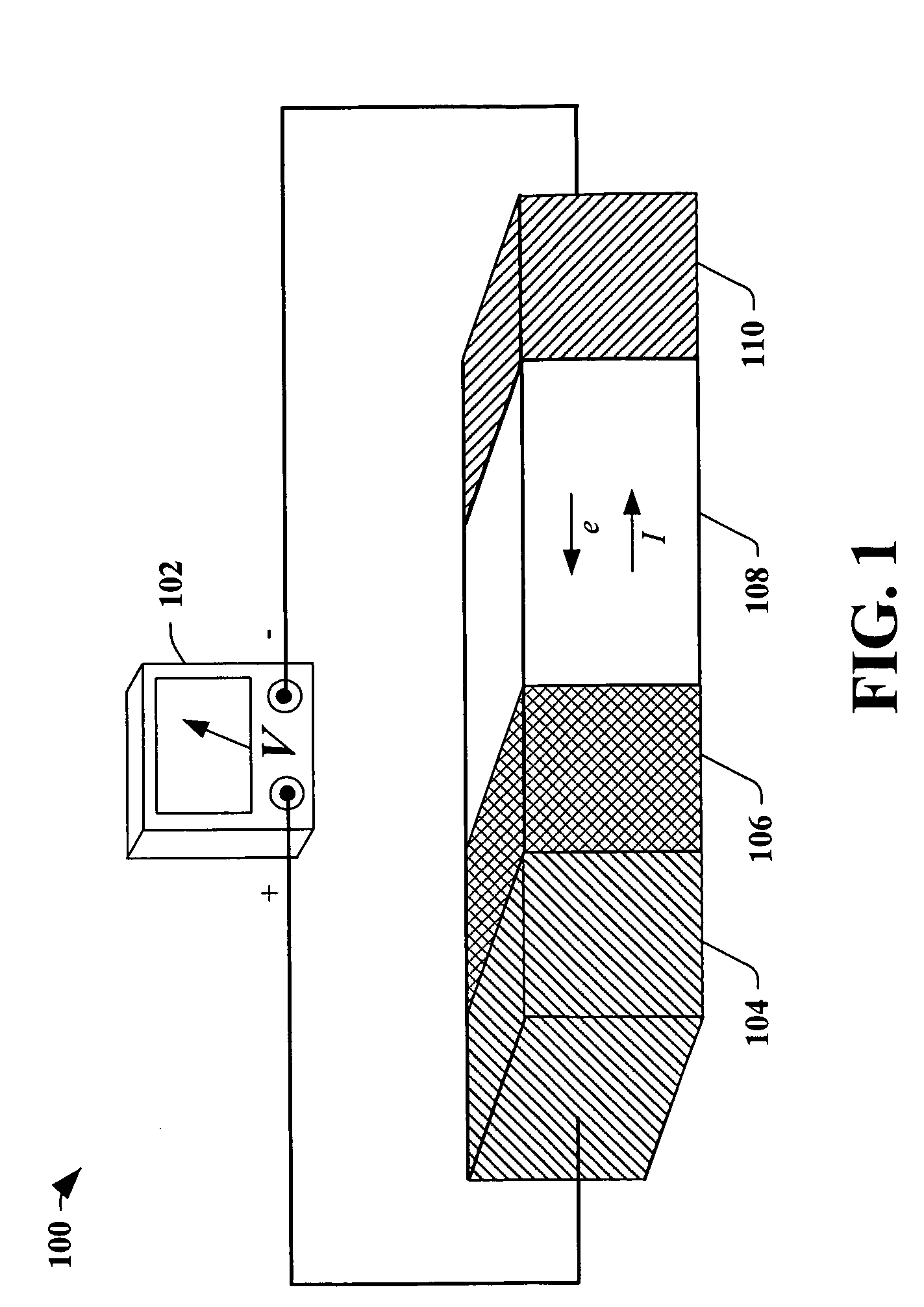
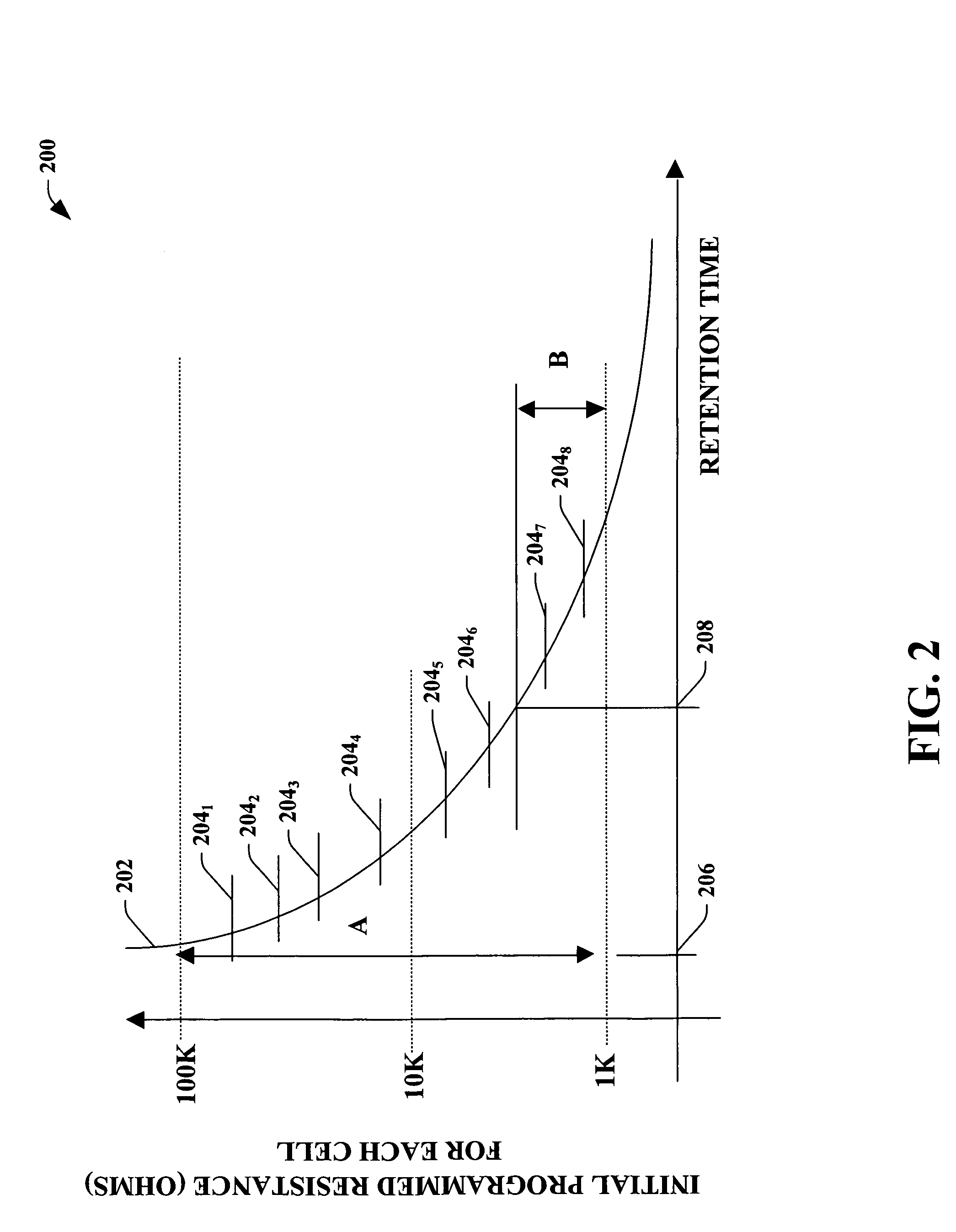
[0035]The present invention is an organic memory device that has the capability to alter its density and level of persistence by changing a resistive state of the organic memory device. The resistive state is changed by applying a voltage potential across an organic memory cell composed of a selectively conductive decay media. A single cell can be set at different resistances to allow multiple bit states per cell which provides a higher device density. At high resistive states, a device's density can be altered in a wide range. For example, at a high resistive state of approximately 10,000 ohms, a single cell can have variable states in a substantially similar order of magnitude with a substantially similar level of persistence. Therefore, the present invention provides higher density memory devic...


PUM


Abstract

An organic memory device comprising two electrodes having a selectively conductive decay media between the two electrodes provides a capability to control a persistence level for information stored in an organic memory cell. A resistive state of the cell controls a conductive decay rate of the cell. A high and / or low resistive state can provide a fast and / or slow rate of conductive decay. One aspect of the present invention can have a high resistive state equating to an exponential conductive decay rate. Another aspect of the present invention can have a low resistive state equating to a logarithmic conductive decay rate. Yet another aspect relates to control of an organic memory device by determining a power state and setting a resistive state of an organic memory cell based upon a current power state and / or an imminent power state.

Description

TECHNICAL FIELD[0001]The present invention relates generally to organic memory devices and, in particular, to organic memory devices with variable persistent memory storage capabilities.BACKGROUND ART[0002]The volume, use and complexity of computers and electronic devices are continually increasing. Computers consistently become more powerful while new and improved electronic devices are continually developed (e.g., digital audio players, video players). Additionally, the growth and use of digital media (e.g., digital audio, video, images, and the like) have further pushed development of these devices. Such growth and development has vastly increased the amount of information desired / required to be stored and maintained for computer and electronic devices.[0003]Generally, information is stored and maintained in one or more of a number of types of storage devices. Storage devices include long term storage mediums such as, for example, hard disk drives, compact disk drives and corresp...

Claims


Application Information

Patent Timeline
Patent Type & Authority Patents(United States)
IPC IPC(8): H01L21/00
CPCG11C11/5664G11C13/0014G11C13/0016G11C13/0035G11C13/0061G11C13/0069G11C14/00H01L27/285G11C2213/55G11C2213/71H10K19/202
Inventor LAN, ZHIDAVAN BUSKIRK, MICHAEL A.FANG, TZU-NINGBILL, COLINENNALS, JOHN S.
Owner MONTEREY RES LLC
Why Eureka
Try Eureka