
Porous silicon composite structure as large filtration array

a composite structure and porous silicon technology, applied in the field of composite microfilters, can solve the problems of reducing the opportunity to introduce fouling during repair, and achieve the effects of reducing or eliminating down time due, reducing or eliminating the time of damage, and being easy to handl

Inactive Publication Date: 2007-10-16
GLOBALFOUNDRIES INC
View PDF39 Cites 31 Cited by
  • Summary
  • Abstract
  • Description
  • Claims
  • Application Information

AI Technical Summary

Benefits of technology

[0015]The present invention is directed to a membrane microfilter having a thin separation layer and a porous silicon substructure, and methods for making the same. The invention is set forth in several embodiments. The present invention offers several important advantages over commercial polymeric membranes. Silicon offers a wide range of materials and surface chemistries for compatibility with a wide range of filtration systems. The 1410° C. melting point of silicon implies that it is a refractory material suitable for higher temperature filtrations; it can also withstand low temperatures. Silicon is relatively inert to chemical attack, except by halogens, alkali solutions, HF and HNO3. Silicon wafers are easy to handle and do not easily tear, crack or suffer other insults during normal handling and use, which significantly reduces or eliminates down time due to repair and reduces the opportunity to introduce fouling during repair. Silicon wafers are not expensive, and are commercially available in 5 inch, 6 inch, 8 inch and 12 inch diameter sizes which can be combined to create large filtration arrays for optimal throughput. Silicon is a suitable support membrane for a polymer that is, or can be modified to be, positively photoactive, or a polymer or inorganic that can be dry etched through a mask.
[0016]A support membrane comprised of other semiconductors such as silicon dioxide, silicon nitride or germanium shares many of the advantages of silicon, including the advantage of handling experience in the microelectronics industry.
[0017]The number of steps in the fabrication of the membrane of the present invention are minimal and are less complex than those known in the art for fabricating membranes, such as phase inversion and phase separation processes. The process of the invention relies on steps commonly practiced using the extant semiconductor processes, clean room facilities and semiconductor tooling used in FEOL / BEOL (Front End of Line / Back End of Line) microelectronics technologies, wherein obtaining features in the submicron range is routine. Fouling is a major concern in the filter art, including fouling that originates in the filter itself. With the simpler, clean, processes and fewer, but more robust materials and process steps of the present invention, cleanliness is favored as fabricated and as cleaned for reuse. Alternatively, the filter is cheap enough to discard after use. It can be implanted in the body. The present invention, which incorporates a lithographic process, can provide a higher packing density than polymer-based structures fabricated by phase inversion or phase separation processes.

Problems solved by technology

Silicon wafers are easy to handle and do not easily tear, crack or suffer other insults during normal handling and use, which significantly reduces or eliminates down time due to repair and reduces the opportunity to introduce fouling during repair.
Fouling is a major concern in the filter art, including fouling that originates in the filter itself.

Method used


Image

  • Porous silicon composite structure as large filtration array
  • Porous silicon composite structure as large filtration array
  • Porous silicon composite structure as large filtration array

Examples


Embodiment Construction

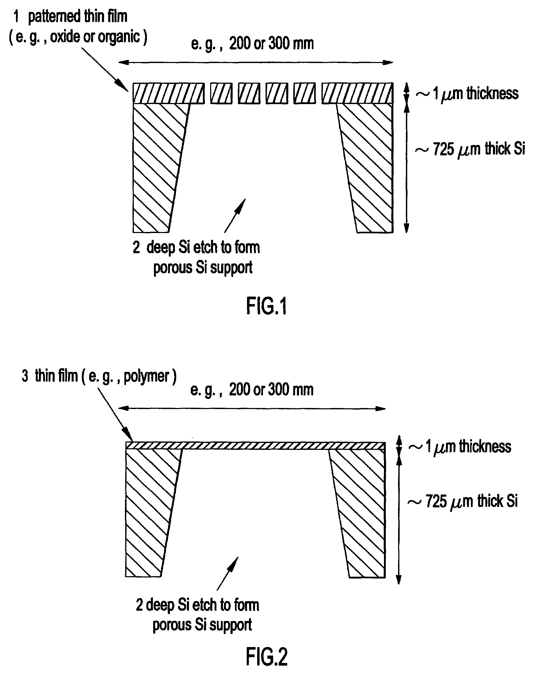
[0021]The filter membrane structure shown in FIG. 1 uses a thin separation layer 1, which can be an inorganic, for example SiO2, or an organic material, that is lithographically patterned by a method known in the art to form a channel-pore structure. A channel-pore structure permits a size-selective process in which molecules larger than the diameter of the channel-pores are retained, while the smaller molecules elute. The thin separation layer 1 is deposited on a bulk crystalline silicon support membrane 2. Spin glass, such as siloxanes, silsesquioxanes, N-silsesquioxanes, and polycabosilanes also can be used to form a separation layer, as can polyimide, polysulfone, and polyethersulfone.

[0022]The silicon material comprises a wafer thickness which, as manufactured, is between about 725 and about 750 μm thick. Thin film separation layer 1 can be deposited by a number of methods known to those skilled in the art, such as chemical vapor deposition (CVD), plasma-enhanced CVD, or spin-o...


PUM

PropertyMeasurementUnit
thickaaaaaaaaaa
thickaaaaaaaaaa
thickaaaaaaaaaa

Abstract

A novel asymmetric filter membrane, and process for making is disclosed in several exemplary versions. The membrane structure is physically robust and suitable for use in a wide variety of applications. The support membrane is may be comprised of material such as a porous silicon or a silicon oxide, and the separation membrane may be comprised of material such as a polymer, zeolite film, or silicon oxide. The process relies on steps adapted from the microelectronics industry.

Description

BACKGROUND[0001]Microfilters are used in separation processes in which solids, liquids or gasses are separated from fluid media. The separation can be on a molecular level or on a coarser level. The present invention relates to the use of a composite microfilter comprising a separation layer and a porous support layer. This type of configuration is known as asymmetric. Aspects of the present invention are conveniently adapted to the art of filtration from processes well established in the art of semiconductor processing.[0002]A simple composite filter typically comprises a thin polymeric membrane separation layer undergirded by a support layer. The separation layer may include very small diameter pores or it may be dense, i.e. essentially opening-free, as in osmotic filtration by absorption and diffusion through a semipermeable membrane. The separation layer may be on the order of about 1-2 microns thick. A thin polymeric layer tends to favor increased permeability, but also tends t...

Claims


Application Information

Patent Timeline
Patent Type & Authority Patents(United States)
IPC IPC(8): B01D39/00B01D29/46B01D53/22B01D67/00B01D69/10B01D69/12B01D71/02B01D71/04
CPCB01D67/0034B01D67/0062B01D67/0072B01D67/0079B01D69/10B01D71/02B01D71/64B01D71/68B01D69/12B01D2325/24B01D2325/022B01D2325/08
Inventor DALTON, TIMOTHY JOSEPHSTEEN, MICHELLE LEIGH
Owner GLOBALFOUNDRIES INC
Learn More