Silicon layer production method and solar cell production method

a solar cell and silicon layer technology, applied in the field of silicon layer, can solve the problems of increasing the cost of substrate, increasing the degree of layer roughening, and large amount of current that cannot be obtained for a final formed solar cell, and achieves the effect of high-performance solar cells and low cos

Inactive Publication Date: 2007-10-16
CANON KK
View PDF43 Cites 4 Cited by
  • Summary
  • Abstract
  • Description
  • Claims
  • Application Information

AI Technical Summary

Benefits of technology

[0009]It is, therefore, an object of the present invention to solve the above-mentioned problem of layer roughening peculiar to a system for effecting LPE growth through the dipping method capable of processing a large number of substrates and to provide an inexpensive and high-performance solar cell.
[0010]To achieve the above object, according to a first aspect of the present invention, there is provided a silicon layer growth method comprising dipping a multicrystalline silicon substrate in a solution comprising silicon and lowering the temperature of the solution, to thereby grow a silicon layer on the substrate, wherein the temperature drop rate of the solution during the dipping of the substrate in the solution is decreased with time.
[0011]Further, according to a second aspect of the present invention, there is provided a solar cell production method comprising the steps of dipping a multicrystalline silicon substrate in a solution comprising silicon and lowering the temperature of the solution, to thereby grow a silicon layer on the substrate; and forming a pn junction in the silicon layer, wherein the temperature drop rate of the solution during the dipping of the substrate in the solution is decreased with time.

Problems solved by technology

However, when a low-cost solar cell is to be attained, this method is not preferable because polishing a surface of a substrate extremely increases the substrate cost.
However, it has been found through experiments by the present inventors that when growing a silicon layer on a multicrystalline silicon substrate etched with a mixed acid by the linear temperature drop LPE growth method, the following problem occurs.
That is, on one hand, a problem occurs that when the growth time is short, although the degree of layer roughening is comparatively small, a large amount of current cannot be obtained for a finally formed solar cell.
On the other hand, when the growth time is long, another problem occurs that although a thick layer is obtained, the degree of layer roughening increases, so that a solar cell is easily shunted (short-circuited) and the fill factor (FF) lowers.
It is apparent that they had no scope to control the LPE layer roughness.
Therefore the temperature profile disclosed in the prior art is not suitable for PV use, which requires a certain amount of a layer thickness for generating enough photocurrent.

Method used


Image

  • Silicon layer production method and solar cell production method
  • Silicon layer production method and solar cell production method
  • Silicon layer production method and solar cell production method

Examples


example 1

(Pretreatment of Substrates)

[0025]Substrates used were metallurgical grade multicrystalline silicon substrates each of 47 mm square and 0.6 mm in thickness. The substrates were cleaned with running water for 5 minutes and then dipped in a mixed liquid of sulfuric acid and hydrogen peroxide solution (3:1 in volume ratio) for 10 minutes. Subsequently, the substrates were cleaned with running water for 5 minutes and then dipped in a mixed liquid of nitric acid, acetic acid and hydrofluoric acid (600:136:64 in volume ratio) for 6 minutes and 30 seconds to etch the surfaces of the substrates. The arithmetical mean surface roughness of the substrate surfaces after the etching ranged between 0.18 μm and 0.43 μm. Finally, the substrates were cleaned with running water for 5 minutes and then dried by dry nitrogen blow, thereby completing the substrate pretreatment.

(Formation of Silicon Layers)

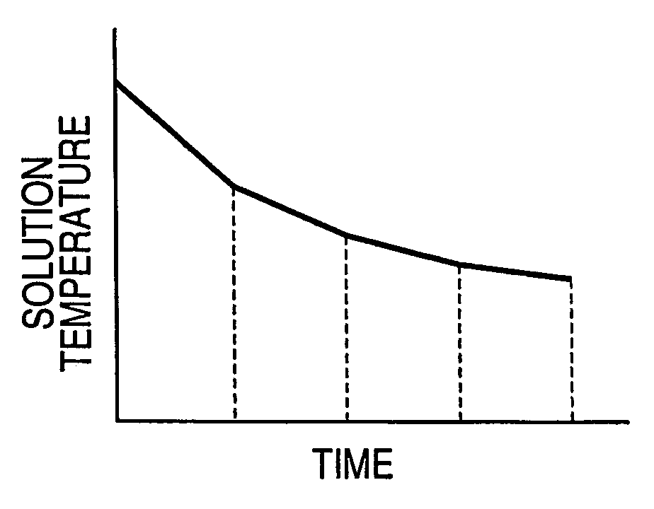
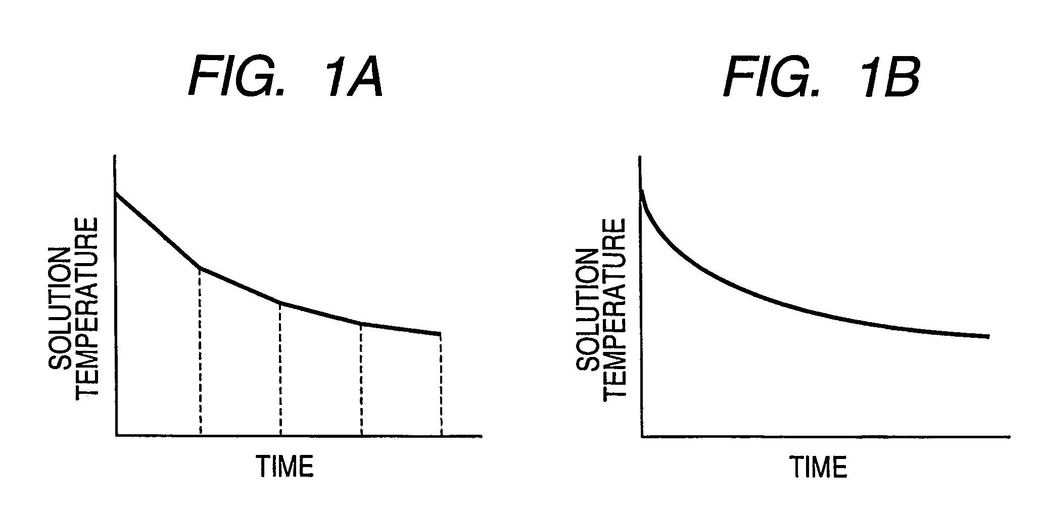
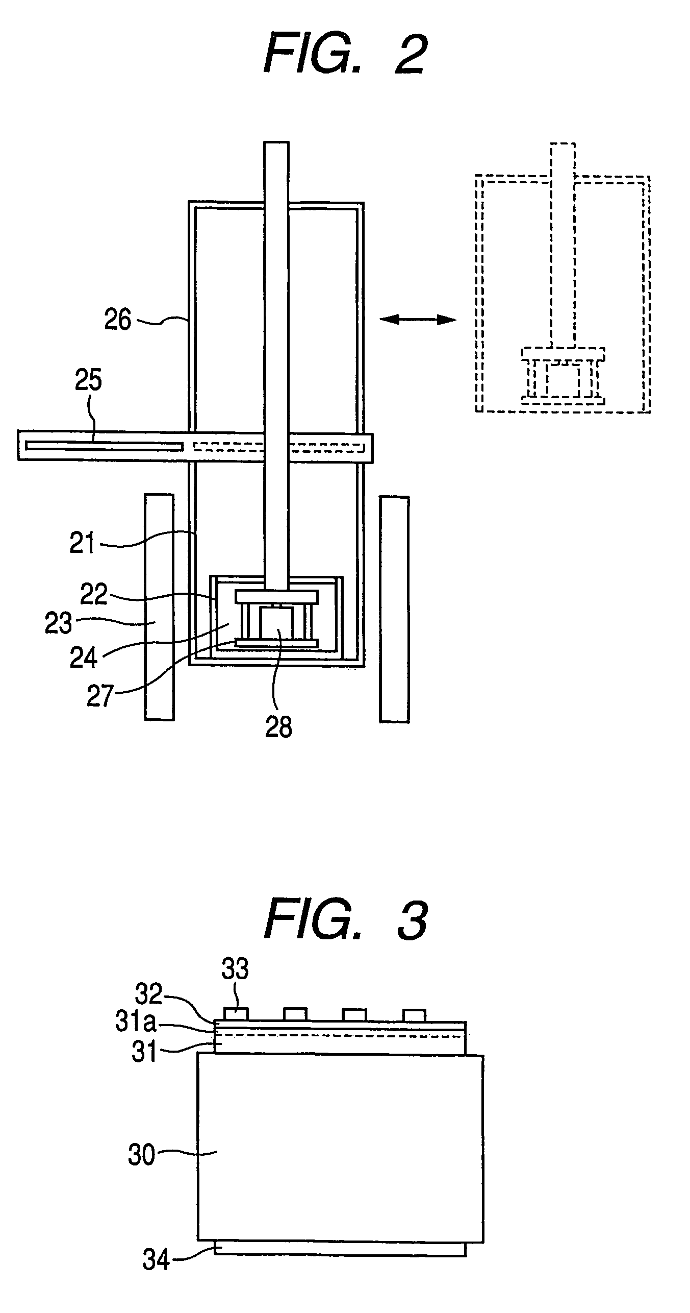
[0026]By using a liquid phase growth apparatus of a structure shown in FIG. 2, a silicon layer was e...


PUM

PropertyMeasurementUnit
surface roughnessaaaaaaaaaa

Abstract

A solar cell is produced by dipping a multicrystalline silicon substrate 28 in a solution 24 containing silicon, growing a silicon layer on the substrate 28 while decreasing with time the temperature drop rate of the solution during the dipping of the substrate in the solution, and forming a pn junction in the silicon layer. Thereby, there is provided a silicon layer production method that can form a thick layer while restraining the degree of roughness, whereby a low-cost, multicrystalline-silicon solar cell production method is provided that realizes both a large current and a high FF.

Description

TECHNICAL FIELD[0001]The present invention relates to a solar cell production method utilizing a silicon layer obtained through a liquid phase growth method.BACKGROUND ART[0002]In order to widely generalize the solar cell, it is necessary to provide an inexpensive solar cell. To reduce the cost, study of various techniques is being progressed at present. As one of the various techniques, Japanese Patent Application Laid-Open No. H11-162859 discloses a technique of growing a high-quality silicon layer on a low-cost multicrystalline silicon substrate containing a comparatively large amount of impurities by a liquid phase epitaxial (LPE) growth method to form a solar cell in the silicon layer. It is expected that this technique reduces the substrate cost of the solar cell. Moreover, it is important, for cost reduction, to improve the photoelectric conversion efficiency of the solar cell. Particularly, it is expected to increase current by means of light trapping effect by providing tex...

Claims


Application Information

Patent Timeline
Patent Type & Authority Patents(United States)
IPC IPC(8): C01B33/26C30B15/20C01B33/02C30B19/02C30B19/10C30B29/06H01L21/208H01L31/04H01L31/18
CPCC30B19/02C30B29/06H01L31/182H01L21/02381H01L21/02658H01L21/02532H01L21/02576H01L21/02579H01L21/02628H01L21/0243Y02E10/546Y02P70/50
Inventor MIZUTANI, MASAKINISHIDA, SHOJINAKAGAWA, KATSUMI
Owner CANON KK
Why Eureka
Try Eureka