Patterned wafer inspection method and apparatus therefor

a technology of patterned wafers and inspection methods, applied in the direction of individual semiconductor device testing, semiconductor/solid-state device testing/measurement, instruments, etc., can solve the problems of reducing the detection reducing the inspection speed or yield of inspection, and reducing the inspection speed. , to achieve the effect of reducing the number of pixels, reducing the number of image data, and simplifying the defect detection process

Active Publication Date: 2007-10-30
HITACHI HIGH-TECH CORP
View PDF9 Cites 17 Cited by
  • Summary
  • Abstract
  • Description
  • Claims
  • Application Information

AI Technical Summary

Benefits of technology

[0011]To guarantee sufficient signal-to-noise ratio that allows meaningful execution of image processing when the beam current value is 100 nA and the resolution is 0.1 μm, the time required to inspect the surface region of a sample having an area of 1 cm2 cannot be reduced to a period shorter than 100 sec.
[0013]It is therefore an object of the present invention to provide a defect inspection method and a defect inspection apparatus that allow high-sensitivity and high-speed detection of an electrically defective portion in a circuit pattern having defects by irradiating an inspection target with a charged particle beam such as an electron beam or an ion beam.
[0017]In addition, the use of the foregoing method allows a reduction in the number of the pixels of an image detector, i.e., a reduction in image data. Since the detection is performed not by a comparison between pattern images which requires image processing but by a magnitude comparison with the set value, a defect detection process can be simplified. As a result, it becomes possible to reduce a burden on an image processing mechanism such as an engine for image processing and significantly increase the speed of defect detection.
[0018]According to the present invention, an inspection method and an inspection apparatus can be implemented which allow, by using an electron beam, high-sensitivity and high-speed inspection of an extremely small opening or an electric defect such as a short circuit or a leakage current in the surface of a sample such as a semiconductor device.

Problems solved by technology

As described above, the SEM defect detection technology has the drawback of a low throughput (inspection speed or yield of inspection).
Moreover, improvement for achieving higher inspection speed has certain limitation, as described herein below.
In a current situation also, the current density of the electron beam has been adjusted to be considerably higher than in the normal SEM but an increase in current density is limited due to the brightness of an electron source, a spatial charge effect, or the like.

Method used


Image

  • Patterned wafer inspection method and apparatus therefor
  • Patterned wafer inspection method and apparatus therefor
  • Patterned wafer inspection method and apparatus therefor

Examples


embodiment 1

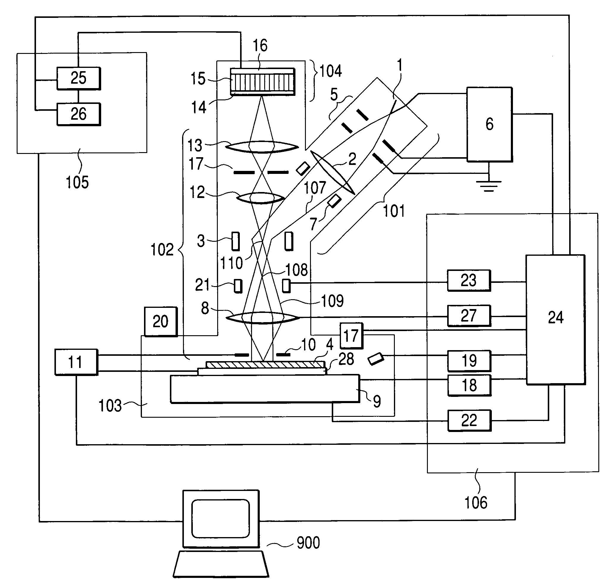
[0028]In the present embodiment, a description will be given to an example in which the present invention is applied to a defect inspection apparatus of a mirror projection (MPJ) type. The description will be given first to the principle of the MPJ and a problem to be solved.

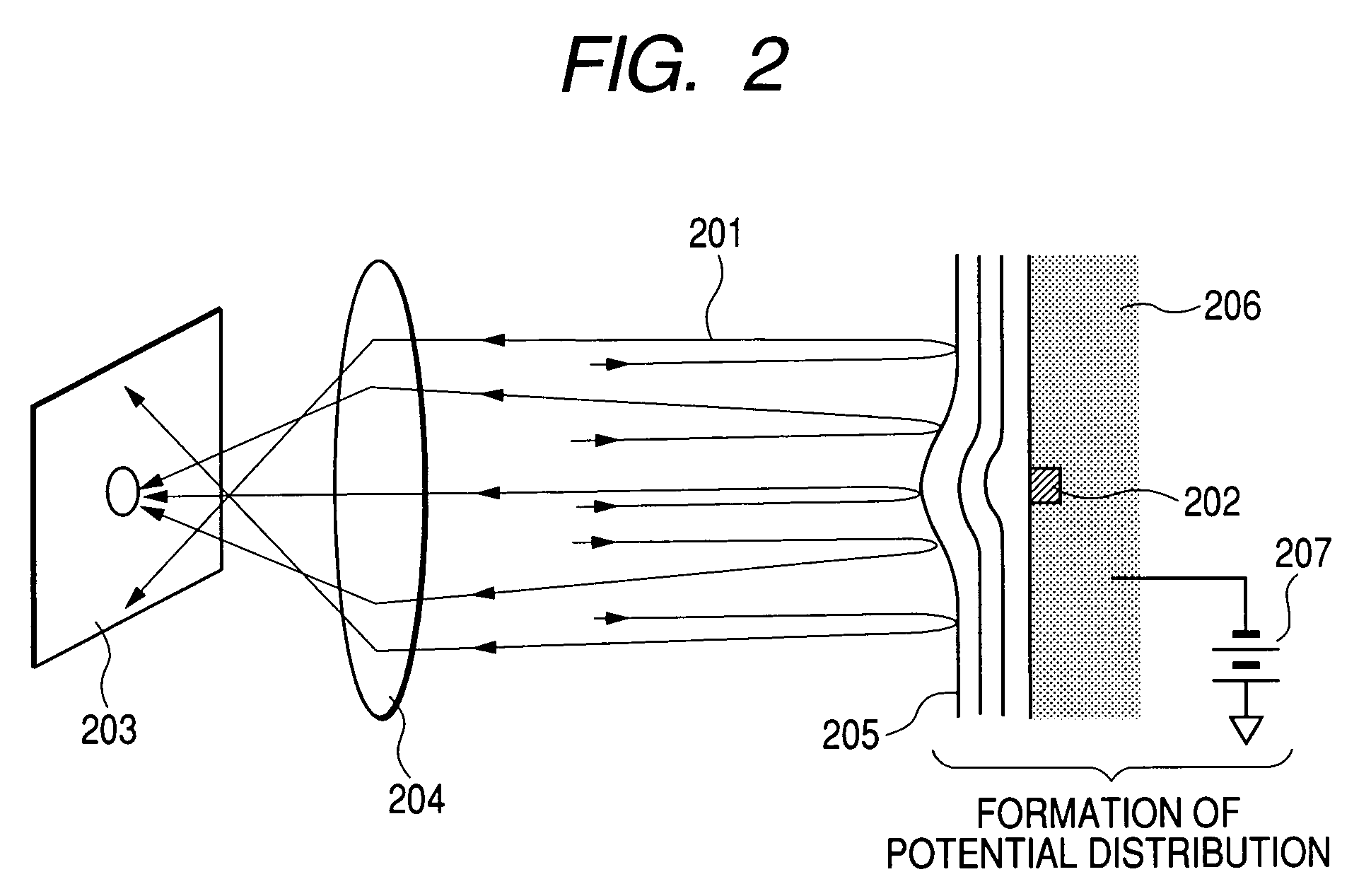
[0029]A consideration will be given to a situation in which the plurality of target regions (areal regions) of a surface of a sample are irradiated with a planar electron beam having a two-dimensional expansion and a negative potential is further applied to a wafer. The negative potential is adjusted to such a value as to return a major part of the electron beam in the vicinity of the outermost surface of the wafer. Specifically, the negative potential is adjusted to a level higher by 0.5 V to 5 V than a potential at an electron source. At this time, the irradiation beam is reflected immediately before the sample and returned by an electric field without colliding with the sample. The electrons will be termed “r...

embodiment 2

[0062]In the first embodiment, the lowest permissible positional accuracy of defect detection has been suppressed to about triple the pattern size or less. To simply detect only the presence or absence of a defect, however, the present invention can be implemented with a simpler structure. In the present invention, what is obtainable as an image is a potential distribution distorted by a defect. Accordingly, there is no image in a normal portion and an image signal is intensified only in a defective portion. If the accuracy required of the location of a defect is not so high, the presence or absence of a defect can be monitored based on the intensity of a whole image instead of obtaining a 2-D intensity distribution of an image.

[0063]In the present embodiment, the size of the irradiated region for one shot is adjusted to about 5 μm and mirror electrons are signalized by using a simple detector for measuring only the magnitude of the intensity of a whole signal. The large difference ...

embodiment 3

[0068]The present embodiment shows an example in which a second SEM tube 801 and the like are provided to enable a detailed defect inspection. FIG. 8 shows a structure thereof. Although the structure shown in the drawing is obtained by adding the SEM tube and the like to the first embodiment, the second embodiment may also be used instead of the first embodiment.

[0069]When particularly detailed observation should be performed with respect to a wafer on which the location of a defect has been determined according to the first embodiment (or the second embodiment), the wafer is transferred to the sample stage 37 under the SEM tube 801 by using a wafer transfer mechanism 36. The wafer transfer mechanism 36 comprises a mechanism capable of transferring the wafer from the sample room 103 to a sample room 802 without bringing the wafer out of the vacuum ambience. In the SEM tube 801, an electron beam 803 emitted from the electron gun 38 forms an extremely small spot on a transferred sampl...


PUM


Abstract

A defect inspection apparatus is provided which allows a technology for inspecting a pattern on a wafer by using an electron beam to implement a high-resolution and higher-speed inspection. A semiconductor wafer is irradiated with an electron beam and electrons reflected in the vicinity of the wafer are detected. The presence or absence of a defect and the location thereof are measured by forming an image from only a component which changes with a periodicity larger than a size of a circuit pattern or the repetition periodicity thereof by using lenses and comparing an image signal with a preset value. Since only the component which changes with a periodicity larger than the size of the circuit pattern with a surface potential distortion and the repetition periodicity thereof is observed with a resolution lower than required to observe the pattern itself instead of detecting a defect through a comparison between extremely small pattern images, an inspection throughput can be increased exponentially compared with that of a conventional SEM inspection.

Description

CLAIM OF PRIORITY[0001]The present application claims priority from Japanese Application JP 2003-426171 filed on Dec. 24, 2003, the content of which is hereby incorporated by reference into this application.FIELD OF THE INVENTION[0002]The present invention relates to a method and apparatus for inspecting an electric defect in an extremely small circuit formed on a semiconductor wafer.BACKGROUND OF THE INVENTION[0003]For the inspection of a defect present in a circuit pattern formed on wafers in a process of manufacturing a semiconductor device, there have been an optical inspection method and an inspection method using a SEM system.[0004]In accordance with the optical inspection method, an image of a surface of a wafer is optically sensed and a defective portion is specified through the analysis of the image. This enables the defect inspection of the wafer surface to be performed at an extremely high speed.[0005]In accordance with the SEM inspection method, a defect present in a cir...

Claims


Application Information

Patent Timeline
Patent Type & Authority Patents(United States)
IPC IPC(8): G01R31/305G01N23/225G21K7/00H01L21/66
CPCG01N23/225H01J37/265H01J37/29H01J2237/24592H01J2237/24585
Inventor HASEGAWA, MASAKIMURAKOSHI, HISAYA
Owner HITACHI HIGH-TECH CORP
Why Eureka
Try Eureka