Fabrication of sub-50 nm solid-state nanostructures based on nanolithography

a solid-state nanostructure and nanolithography technology, applied in nanoinformatics, photomechanical equipment, instruments, etc., can solve the problems of expensive equipment used in electron beam lithography, and achieve the effect of high resolution

Inactive Publication Date: 2007-11-06
NORTHWESTERN UNIV
View PDF2 Cites 105 Cited by
  • Summary
  • Abstract
  • Description
  • Claims
  • Application Information

AI Technical Summary

Problems solved by technology

Electron beam lithography is done with expensive equipment as well.

Method used


Image

  • Fabrication of sub-50 nm solid-state nanostructures based on nanolithography
  • Fabrication of sub-50 nm solid-state nanostructures based on nanolithography
  • Fabrication of sub-50 nm solid-state nanostructures based on nanolithography

Examples


working example 1

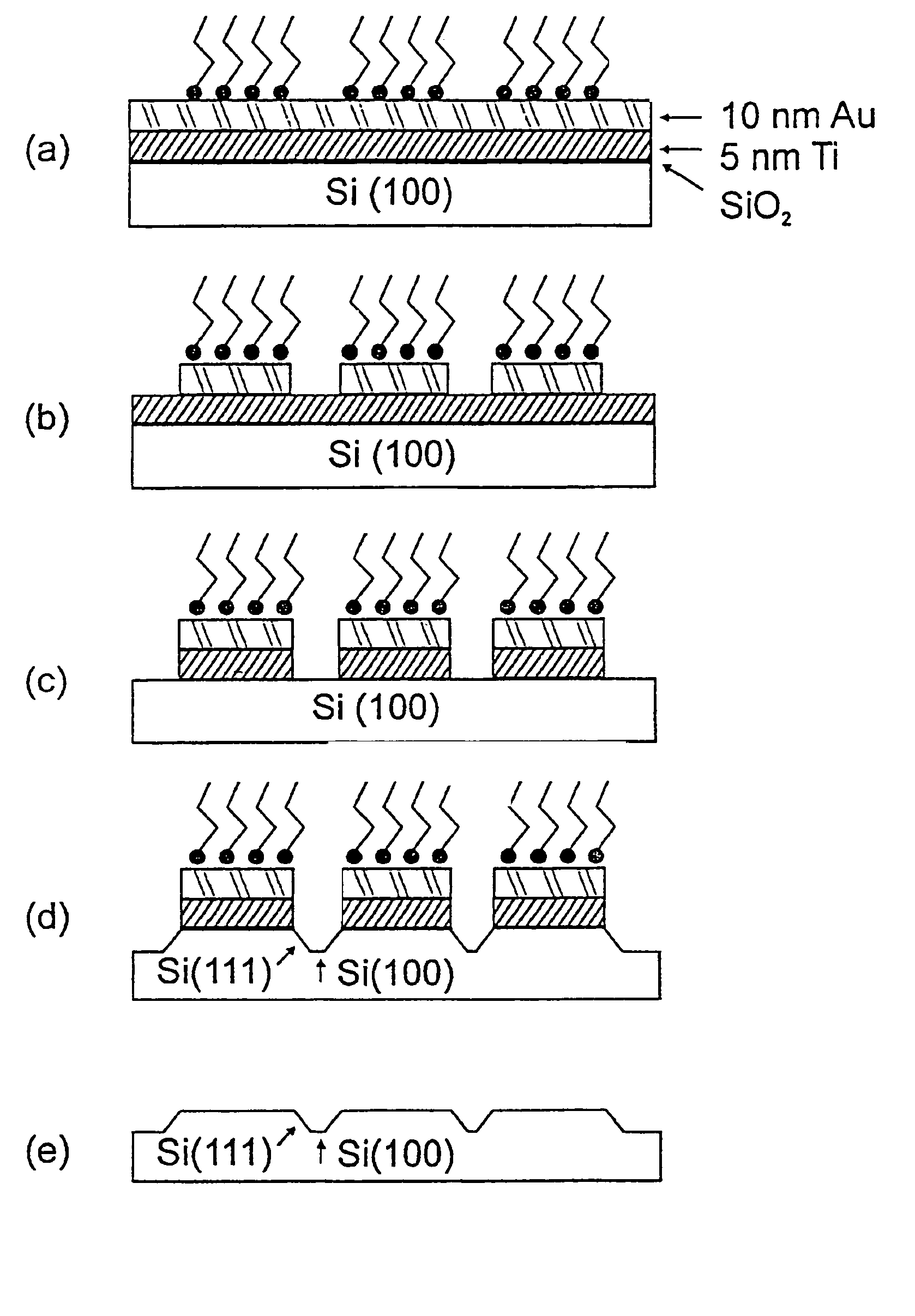
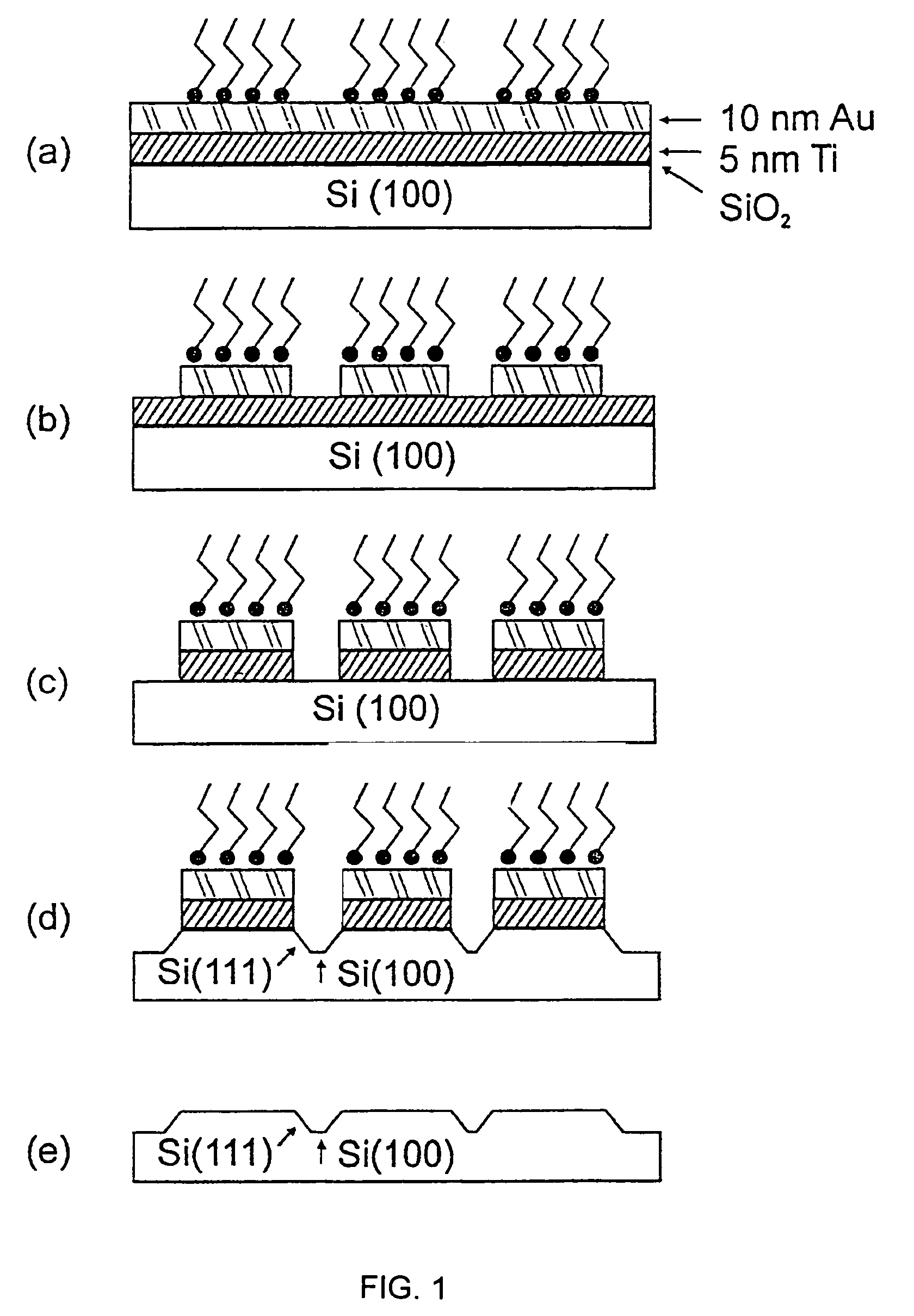
[0072]Introductory description for the working example is provided, supplementing the above introductory description. Lithographic techniques such as photolithography (Wallraff and Hinsberg, Chem. Rev., 99:1801 (1999)), electron beam lithography (Wallraff and Hinsberg, Chem. Rev., 99:1801 (1999); Xia et al., Chem. Rev., 99:1823 (1999)), and microcontact printing (Xia et al., Chem. Rev., 99:1823 (1999)) can be used with varying degrees of ease, resolution, and cost to generate three-dimensional features on silicon wafers. DPN is complementary to other aforementioned nanolithographic techniques, but can be used with conventional laboratory instrumentation (an AFM), in routine fashion, to generate patterns of alkylthiols on polycrystalline gold substrates under ambient conditions. Moreover, DPN offers 15 nm linewidth and 5 nm spatial resolution with conventional AFM cantilevers. (see prior examples, Piner et al., Science, 283:661 (1999); Piner et al., Langmuir, 15:5457 (1999); Hong et ...

working example 2

[0092]In a typical experiment, gold-coated (10 nm), Ti-coated (1 nm) silicon oxide (Au / Ti / SiOx / Si) (references 6a,b) was patterned via DPN™ printing with 16-mercaptohexadecanoic acid (MHA) using a Park Scientific CP AFM (Thermomicroscopes, Sunnyvale, Calif.) and commercial lithography software (DPNWrite™, DPN System-1, NanoInk Inc., Chicago, Ill.) (references 5, 6a,b). All patterning experiments were carried out under ambient conditions (set point=0.5 Nn, 24-26° C., 44-49% relative humidity) with a MHA-coated tip, which was prepared by immersing a Si3N4 tip (spring constant=0.05 N / m, Thermomicroscopes, Sunnyvale, Calif.) in an acetonitrile solution saturated with MHA for ˜5 s with subsequent drying with compressed difluoroethane (Dust-off, Ted Pella, Inc., Redding, Calif.). Each DPN dot feature was generated by holding a MHA-coated tip in contact with an Au surface for 0.01 s (i.e., a holding time), and each line was generated by moving a MHA-coated tip on an Au surface at a constan...

working example 3

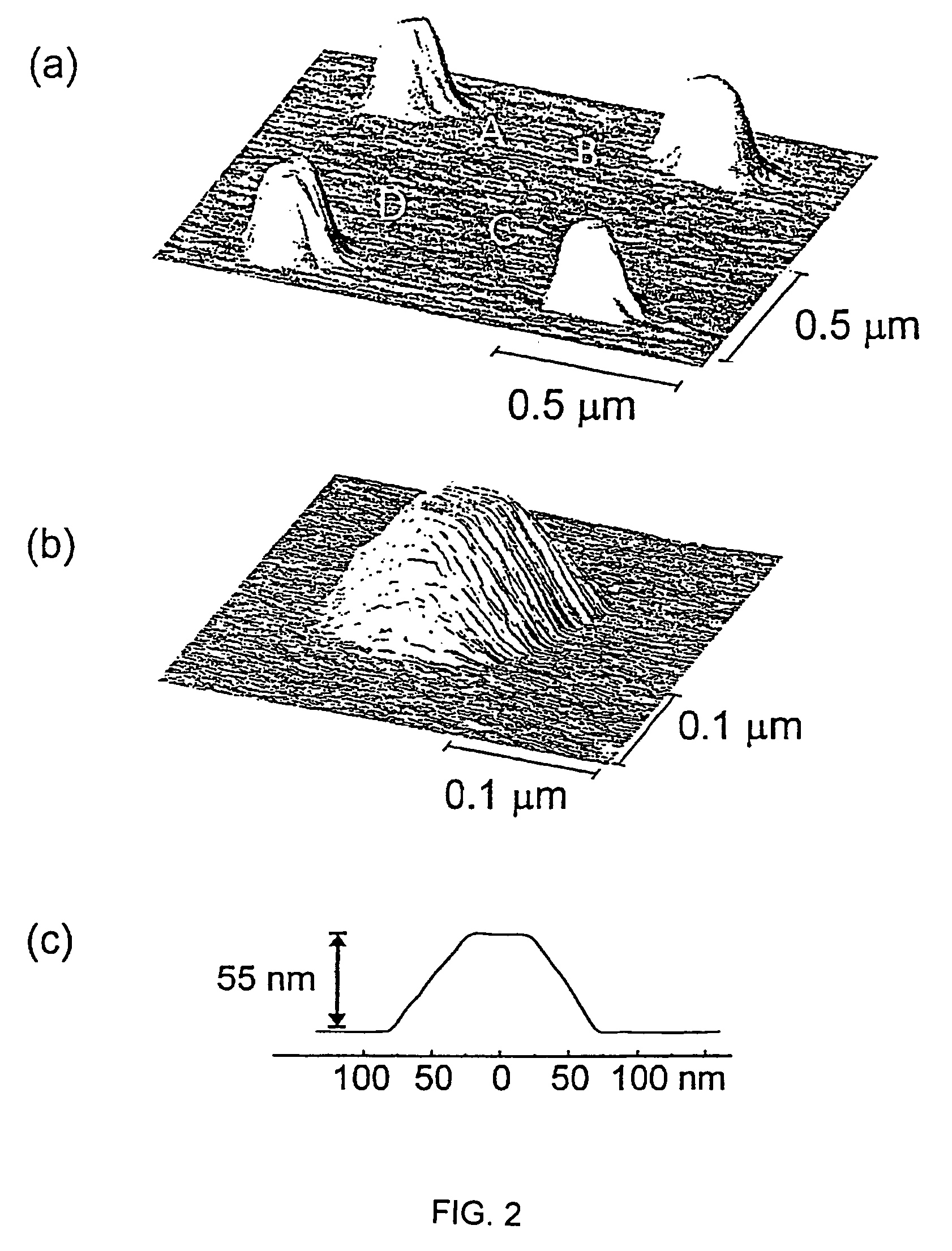
[0095]In a typical experiment, 20 μm long lines of MHA were generated by moving a MHA-coated tip on an Au surface at a rate 0.5 (FIG. 7A), 0.25 (FIG. 7B), and 0.25 (FIG. 7C) μm / s with a designed gap distance of 100 (FIG. 7A), 90 (FIG. 7B), and 20 nm (FIG. 7C), respectively. After etching the exposed areas of the Au film with a ferri / ferrocyanide etchant (reference 6a), TMAFM images show that the measured sizes of the obtained nanogaps are ˜97 (FIG. 7A), 82 (FIG. 7B), and 12 (FIG. 7C) nm (see FIGS. 10-12 for section analysis), respectively. The obtained gap sizes are a little smaller than the designed gap sizes, possibly a consequence of MHA diffusion, which in some cases may not be fully accounted for in the software or experimental protocol, and which in some cases may not take into account differences in the ink diffusion as a function of tip coating. The widths of the etched lines are about 70 (FIG. 7A), 170 (FIG. 7B) and 165 (FIG. 7C) nm, respectively. These data show that one c...


PUM

PropertyMeasurementUnit
distancesaaaaaaaaaa
distancesaaaaaaaaaa
deposition timeaaaaaaaaaa

Abstract

Combination of nanolithography and wet chemical etching including the fabrication of nanoarrays of sub-50 nm gold dots and line structures with deliberately designed approximately 12-100 nm gaps. These structures were made by initially using direct write nanolithography to pattern the etch resist, 16-mercaptohexadecanoic acid (MHA), on Au / Ti / SiOx / Si substrates and then wet chemical etching to remove the exposed gold. These are the smallest Au structures prepared by a wet chemical etching strategy. Also, Dip-Pen Nanolithography (DPN) has been used to generate resist layers on Au, Ag, and Pd that when combined with wet chemical etching can lead to nanostructures with deliberately designed shapes and sizes. Monolayers of mercaptohexadecanoic acid (MHA) or octadecanethiol (ODT), patterned by DPN, were explored as etch resists. They work comparably well on Au and Ag, but ODT is the superior material for Pd. MHA seems to attract the FeCl3 etchant and results in nonuniform etching of the underlying Pd substrate. Dots, lines, triangles and circles, ranging in size from sub-100 to several hundred nm have been fabricated on these substrates. These results show how one can use DPN as an alternative to more complex and costly procedures like electron beam lithography to generate nanostructures from inorganic materials.

Description

DESCRIPTION OF RELATED APPLICATIONS[0001]This application claims benefit of provisional application 60 / 430,349 to Zhang et al. filed Dec. 3, 2002 (“Fabrication of Sub-50 nm Solid State Nanostructures Based on Nanolithography”), which is hereby incorporated by reference in its entirety. This application also is a continuation-in-part of U.S. application Ser. No. 09 / 866,533 filed May 24, 2001 now U.S. Pat. No. 6,827,979 to Mirkin et al, which is hereby incorporated by reference in its entirety, and which claims priority to provisional application No. 60 / 207,713 filed May 26, 2000, all of which are incorporated by reference in their entirety.STATEMENT OF GOVERNMENT SUPPORT[0002]This work was supported by the Federal Government under Grant No. F49620-00-1-0283 / PO1 from the Air Force Office of Scientific Research; DAAD 19-00-1-0414 from DARPA; and EEC-0118025 from the National Science Foundation. The government may have certain rights in the invention.INTRODUCTION[0003]Nanolithography co...

Claims


Application Information

Patent Timeline
Patent Type & Authority Patents(United States)
IPC IPC(8): B44C1/22C03C15/00C03C25/68C23F1/00
CPCB82Y10/00B82Y40/00G03F7/2049G03F7/0002B82Y30/00Y10T428/24917Y10T428/24802
Inventor MIRKIN, CHAD A.ZHANG, HUAWEINBERGER, DANAHONG, SEUNGHUN
Owner NORTHWESTERN UNIV
Why Eureka
Try Eureka