
QWIP with tunable spectral response

a spectral response and spectral response technology, applied in the field of tunable qwip focal plane array, can solve the problem that there is no device capable of performing the like of target imaging at the fpa level, and achieve the effect of effective operation and facilitation of absorption

Inactive Publication Date: 2007-11-06
MIND FUSION LLC
View PDF23 Cites 10 Cited by
  • Summary
  • Abstract
  • Description
  • Claims
  • Application Information

AI Technical Summary

Benefits of technology

[0009]One embodiment of the present invention provides a tunable quantum well infrared photodetector focal plane array (QWIP FPA) imaging device. The device includes one or more detector layers configured with asymmetric quantum wells. Each detector layer is between contact layers, thereby defining a stack of layers having a front side and a back side. Each detector layer has a spectrum of light absorption that changes in response to an applied bias. Thus, each detector layer can effectively operate as a tunable channel. For example, applying a first bias causes a first spectrum of absorption to be dominant and applying a second bias causes a second spectrum of absorption to be dominant. A light-coupling grating is formed on the backside of the stack. The grating has a pattern that reflects a substantial portion of incoming light so as to disperse that light through the one or more of the detector layers, thereby facilitating absorption. A reflective coating on the sides of the detector layers provides, in conjunction with the light-coupling grating, a photon-in-a-box configuration for containing light. Note that the stack of layers can be one multicolor pixel of the device that is repeated a number of times, thereby defining an array of the multicolor pixels.
[0010]Each detector layer can be configured to have a thickness of about one micron or less. The device may further include a read-out integrated circuit (ROIC) that includes biasing circuitry adapted to deliver bias signals to each detector layer thereby enabling tunability of the corresponding spectrum of light absorption. Coarse tuning could be used, for example, to cause bimodal spectral shifts (e.g., from mid-wavelength IR to long-wavelength IR), while fine tuning could be used to cause smaller spectral shifts within a particular mode (e.g., for spectroscopy applications). In one particular such embodiment, each contact layer of the device is electrically coupled to a backside contact, thereby facilitating connection to the ROIC. The ROIC may further include an image processor adapted to receive pixel data from each detector layer and to generate corresponding images associated with the pixel data. In another such embodiment, each asymmetric quantum well is a unit cell comprising two quantum wells coupled by a barrier. One of the quantum wells is configured to absorb a first spectrum, and the other quantum well is configured to absorb a second spectrum. Applying a first bias causes the first spectrum to be dominant and applying a second bias causes the second spectrum to be dominant. The quantum well configured to absorb the second spectrum may include a well spike, which effectively raises the ground state of that well.
[0012]The device may further be configured with a read-out integrated circuit (ROIC) that includes biasing circuitry adapted to deliver the first and second bias signals to each detector layer, thereby enabling spectral tunability of the device. Each contact layer of the device can be electrically coupled to a backside contact, thereby facilitating connection to the ROIC. The ROIC may further include an image processor adapted to receive pixel data from each detector layer, and to generate corresponding images associated with the pixel data. Note that the stack of layers can be one multicolor pixel of the device, and repeated a number of times thereby defining an array of the multicolor pixels. Each pixel can provide pixel data to the image processor.

Problems solved by technology

Such functionality is not trivial, and is associated with a number of difficult implementation problems.
In addition, although various tunable absorption schemes have been developed, where the wavelength of absorption is tunable (e.g., such as those using asymmetric quantum wells), there appears to be no device that is capable of tunability at the FPA level for performing the likes of target imaging.

Method used


Image

  • QWIP with tunable spectral response
  • QWIP with tunable spectral response
  • QWIP with tunable spectral response

Examples


Embodiment Construction

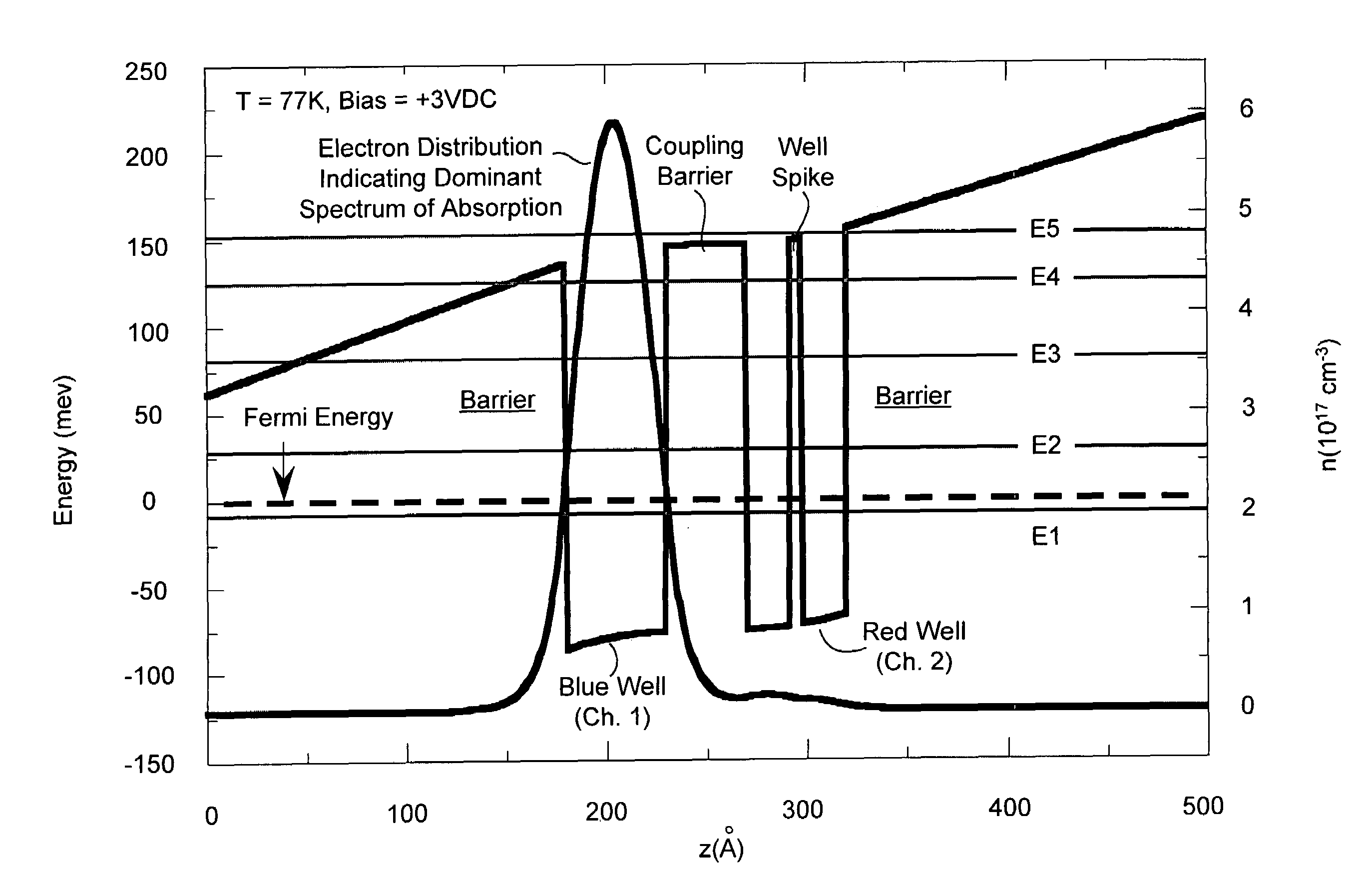
[0026]Embodiments of the present invention provide a tunable QWIP FPA device that is configured for multi-modal and spectral tunability for performing the likes of imaging and spectroscopy. A selected bias voltage is applied across the contacts associated with a particular detector layer or “channel” of the device, where each applied bias corresponds to a particular target spectrum for detection. Each detector layer has a spectral response that can be coarse tuned for a bimodal or dual-band operation (e.g., MW / LW). Also, each detector layer is configured for continuous or fine tuning within a particular mode (e.g., MW / MW). Thus, dynamic bias-controlled tuning is enabled.

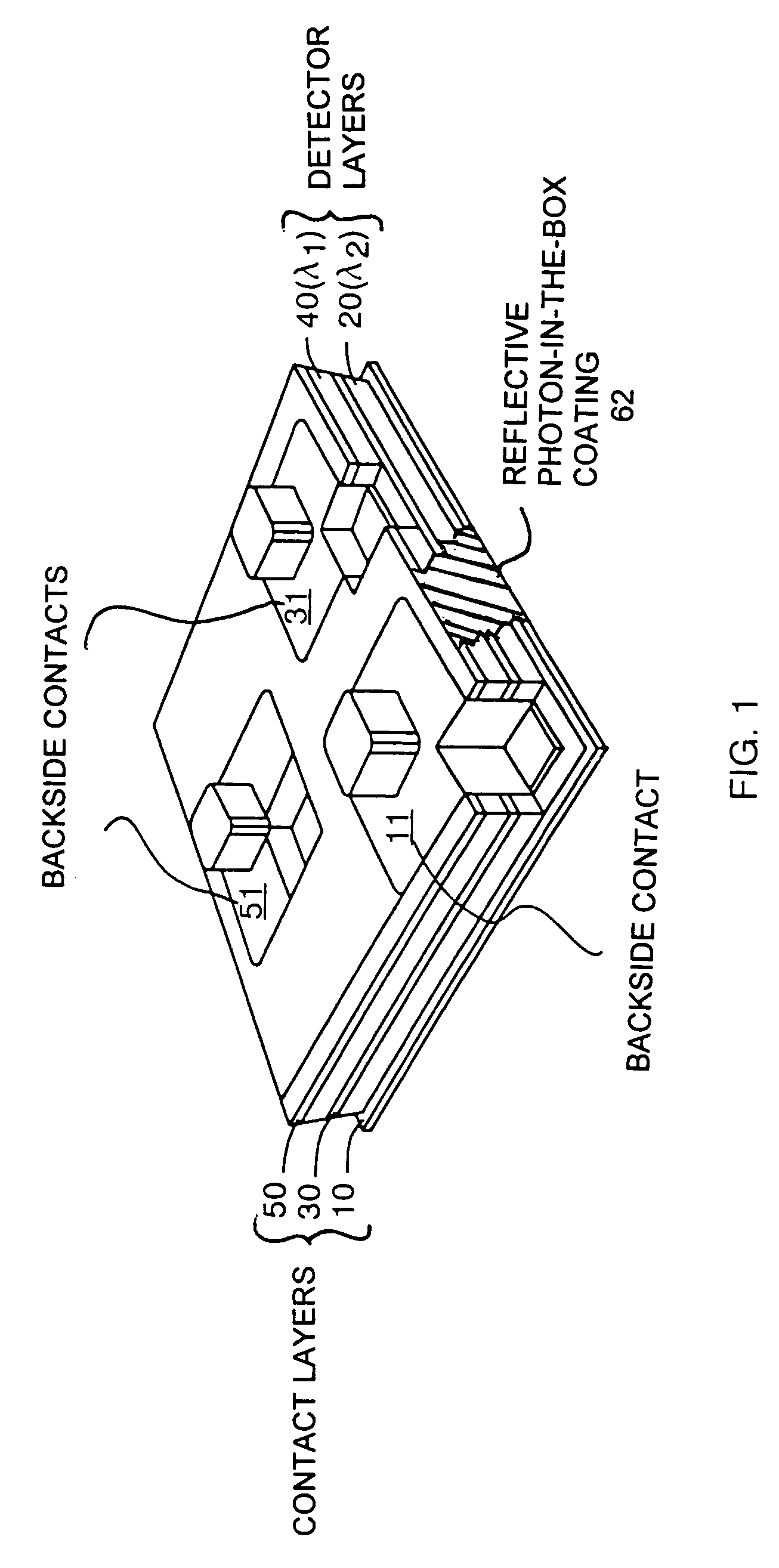
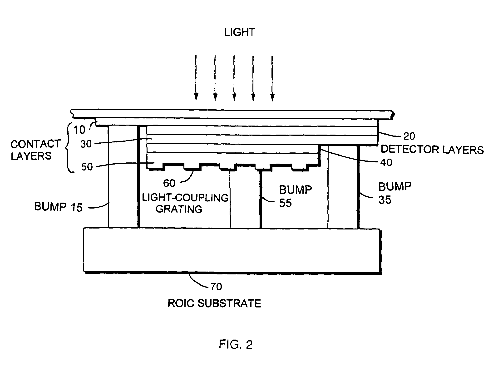
[0027]The tunable QWIP FPA can be fabricated as a multifocal plane imaging device using conventional epitaxial growth techniques on a substrate. Back side contacts can be used to enable direct, discrete, pixel to ROIC connection and direct current readout for each detected wavelength (i.e., per channel). Each detecto...


PUM


Abstract

A tunable QWIP FPA device that is configured for spectral tunability for performing the likes of imaging and spectroscopy is disclosed. A selected bias voltage is applied across the contacts associated with a particular detector layer / channel of the device, where each applied bias corresponds to a particular target spectrum / color for detection. Each detector layer / channel can be coarse tuned for a bimodal or dual-band operation (e.g., MWIR / LWIR). Also, each detector layer / channel is configured for continuous or fine tuning within a particular mode (e.g., MWIR / MWIR). Thus, dynamic bias-controlled tuning is enabled. Asymmetric quantum well configurations enable this tunability.

Description

RELATED APPLICATIONS[0001]This application is a continuation-in-part of U.S. patent application Ser. No. 09 / 746,956, filed Dec. 22, 2000 now U.S. Pat No. 6,875,975, which claims the benefit of U.S. Provisional Application No. 60 / 173,077, filed Dec. 24, 1999. This application is also a continuation-in-part of U.S. patent application Ser. No. 10 / 781,523, filed Feb. 18, 2004 now U.S. Pat. No. 7,238,960. Each of these applications is herein incorporated in its entirety by reference.FIELD OF THE INVENTION[0002]The invention relates to quantum well infrared photodetector (QWIP) technology, and more particularly, to a tunable QWIP focal plane array capable of multiple dual-band imaging.BACKGROUND OF THE INVENTION[0003]A quantum well designed to detect infrared (IR) light is called a quantum well infrared photodetector (QWIP). QWIPs operate by photo-excitation of electrons between a ground state and an excited state of its quantum wells. In more detail, a quantum well absorbs IR photons. Th...

Claims


Application Information

Patent Timeline
IPC IPC(8): H01L31/0304G01J3/28G01J5/00H01L27/146H01L29/06H01L31/0203H01L31/0352H01L31/101
CPCB82Y20/00G01J3/2803H01L27/1465H01L27/14652H01L31/02161H01L31/03046H01L31/0352H01L31/035236H01L31/101H01L31/0232Y02E10/544H01L31/02327H01L31/1013
Inventor SUNDARAM, MANIREISINGER, AXEL R
Owner MIND FUSION LLC
Learn More