Method of making a metal-insulator-metal capacitor in the CMOS process

a metal-insulator and metal-based technology, applied in capacitors, semiconductor devices, semiconductor/solid-state device details, etc., can solve the problems that the process flow of making a polysilicon to polysilicon or a polycide to polycide capacitor is not transparent to present or future cmos technology, and achieves low resistance

Inactive Publication Date: 2007-11-13
TAIWAN SEMICON MFG CO LTD
View PDF13 Cites 41 Cited by
  • Summary
  • Abstract
  • Description
  • Claims
  • Application Information

AI Technical Summary

Benefits of technology

[0012]Yet another object is to provide a method for fabricating a metal-insulator-metal capacitor having low resistivity.

Problems solved by technology

The process flow for making a polysilicon to polysilicon or polycide to polycide capacitor is not transparent to present or future CMOS technology.

Method used


Image

  • Method of making a metal-insulator-metal capacitor in the CMOS process
  • Method of making a metal-insulator-metal capacitor in the CMOS process
  • Method of making a metal-insulator-metal capacitor in the CMOS process

Examples


Embodiment Construction

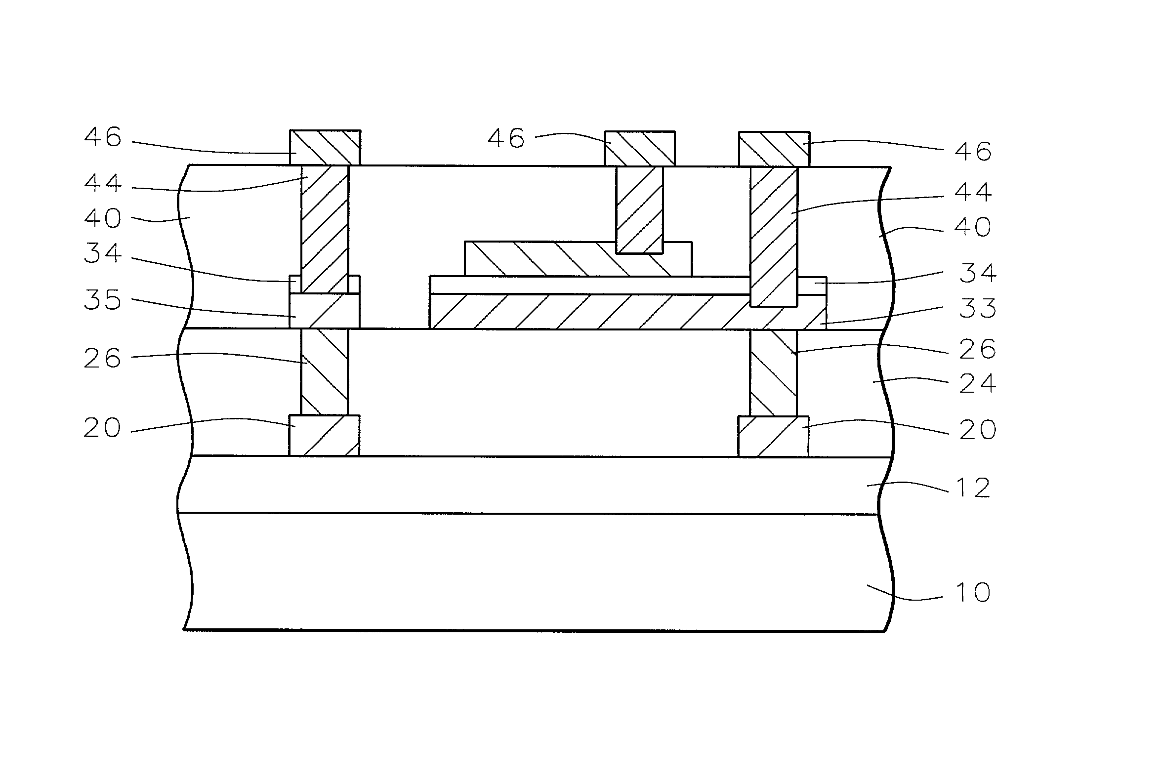
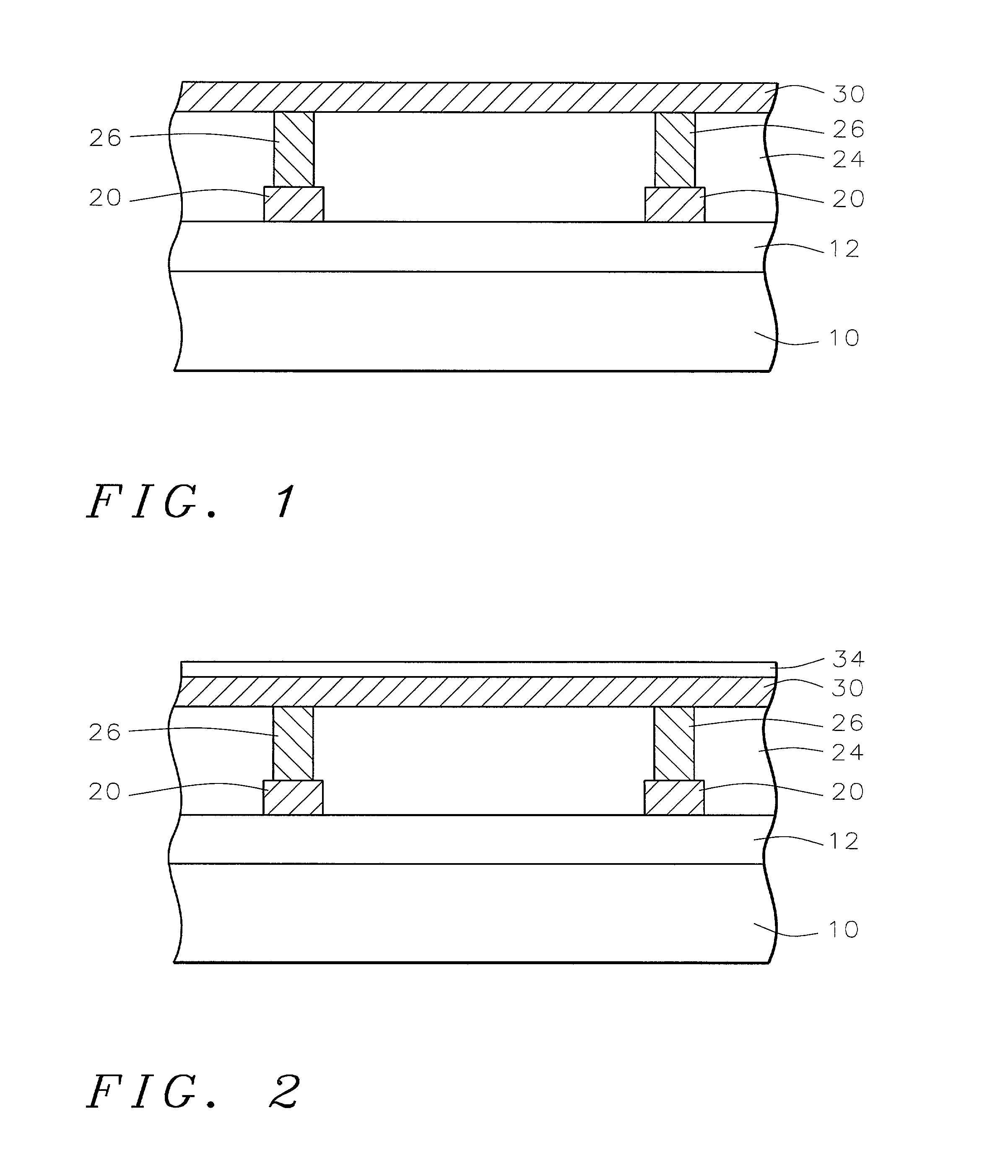
[0017]Referring now more particularly to FIG. 1, there is shown a partially completed integrated circuit device. The semiconductor substrate 10 is preferably composed of silicon having a (100) crystallographic orientation. Semiconductor device structures are formed in and on the semiconductor substrate. These may include gate electrodes and interconnection lines and associated source and drain regions and lower level metal lines. The semiconductor device structures, not shown, may be formed in layer 12 and covered with an insulating layer.

[0018]Next, metal lines 20 are formed as is conventional in the art. A thick insulating layer, such as chemically vapor deposited (CVD) silicon dioxide, phosphosilicate glass (PSG), high density plasma oxide, or the like, 24 is deposited over the lines 20 and then planarized, for example by chemical mechanical polishing (CMP), to obtain a flat surface.

[0019]Using conventional lithographic and etching techniques, via or contact openings are made thr...


PUM

PropertyMeasurementUnit
thicknessaaaaaaaaaa
thicknessaaaaaaaaaa
thicknessaaaaaaaaaa

Abstract

A method for fabricating an improved metal-insulator-metal capacitor is achieved. An insulating layer is provided overlying conducting lines on a semiconductor substrate. Via openings through the insulating layer to the conducting lines are filled with metal plugs. A first metal layer is deposited overlying the insulating layer and the metal plugs. A capacitor dielectric layer is deposited overlying the first metal layer wherein capacitor dielectric layer is deposited as a dual layer, each layer deposited within a separate chamber whereby pinholes are eliminated. A second metal layer and a barrier metal layer are deposited overlying the capacitor dielectric layer. The second metal layer and the barrier metal layer are patterned to form a top plate electrode. Thereafter, the capacitor dielectric layer and the first metal layer are patterned to form a bottom plate electrode completing fabrication of a metal-insulator-metal capacitor.

Description

BACKGROUND OF THE INVENTION[0001](1) Field of the Invention[0002]The present invention relates to a method of fabricating a metal-insulator-metal capacitor, and more particularly, to a method of forming an improved metal-insulator-metal capacitor in the fabrication of an integrated circuit device.[0003](2) Description of the Prior Art[0004]Capacitors are critical components in the integrated circuit devices of today. Both polysilicon-insulator-polysilicon and metal-insulator-metal (MIM) capacitors have been used in the art. Polysilicon to polysilicon or polycide to polycide (PIP) capacitors perform at a high parasitic capacitance. Parasitic capacitance is calculated as the ratio of the Ccapacitor to Csubstrate, where Ccapacitor is the capacitance between the capacitor plates and Csubstrate is the capacitance between the top plate or bottom plate of the capacitor to the silicon substrate. Generally, the parasitic capacitance for PIP capacitors is about 10%, but for MIM capacitors, th...

Claims


Application Information

Patent Timeline
Patent Type & Authority Patents(United States)
IPC IPC(8): H01L21/336
CPCH01L21/8221H01L28/75H01L23/5223H01L2924/0002
Inventor HO, YEN-SHIHCHUNG, JAU-YUANNCHEN, CHUN-HONTAO, HUN-JAN
Owner TAIWAN SEMICON MFG CO LTD
Why Eureka
Try Eureka