Field emission lighting device

a field emission and lighting device technology, applied in the field of electronic lighting technology, can solve problems such as virtually stalled progress, and achieve the effects of good young's modulus, good mechanical strength, and excellent field emission capability

Inactive Publication Date: 2007-11-27
HON HAI PRECISION IND CO LTD
View PDF4 Cites 0 Cited by
  • Summary
  • Abstract
  • Description
  • Claims
  • Application Information

AI Technical Summary

Benefits of technology

[0008]Each of the molybdenum tips may be closely combined with the emitter base. Because the combined molybdenum tips and the emitter base have good mechanical strength, excellent field-emission capability and good Young's modulus, the combined molybdenum tips and the emitter base can be subjected to relatively high voltage electrical fields without being damaged.
[0009]A high voltage electrical field may ensure a high current of field emission. The high current of field emission gives the lighting device a high luminosity, with visible light having satisfactory brightness being obtained. Therefore the lighting device and the lighting device with the molybdenum tips and the emitter base may emit light having relatively high brightness. The brightness is about 10 to about 1000 times that of a comparable light emitting diode (LED) or high intensity discharge (HID) lamp.

Problems solved by technology

However, the progress appears to have virtually stalled in recent years.

Method used


Image

  • Field emission lighting device
  • Field emission lighting device
  • Field emission lighting device

Examples


Embodiment Construction

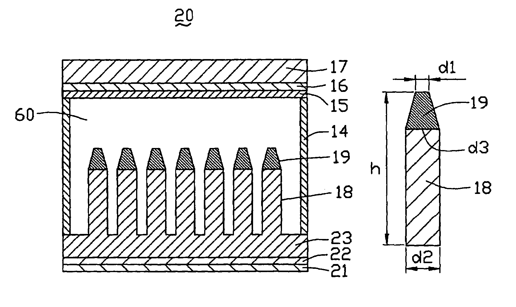
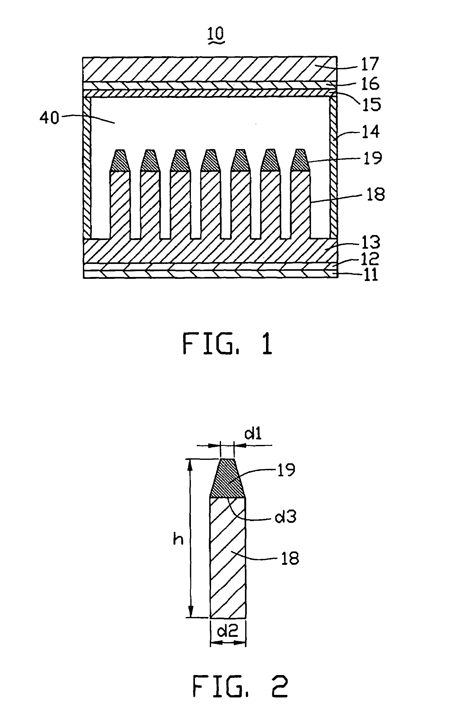
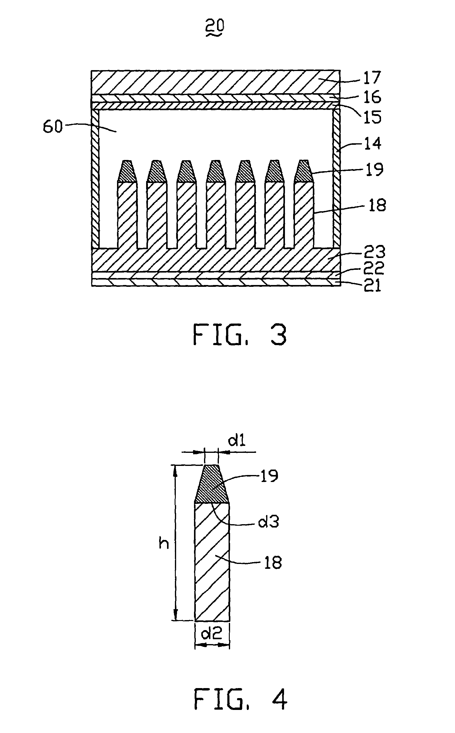
[0016]Referring to FIG. 1, a first preferred embodiment provides a lighting device 10 including a substrate (not shown), a cathode 11, a cover 12, an insulation layer 13, at least one silicon nitride base 18, one or more molybdenum tips 19, a phosphor layer 15, an anode 16, a sidewall 14, and a silicon oxide (SiO2 or SiOx) layer 17.

[0017]The substrate may be made of a metal or metal alloy. The metal may be silver (Ag) or copper (Cu). Such metal or metal alloy substrate may be smooth, to facilitate formation of the cathode 11.

[0018]The cathode 11 formed on the substrate may be an electrically conductive material selected from the group consisting of copper (Cu), silver (Ag), and gold (Au). The cathode 11 is preferably formed to have a thickness of less than 1 micrometer.

[0019]The cover 12 may be a silicon layer formed by a depositing process. The formed cover 12 may serve as a nucleation layer on the cathode 11. The nucleation layer may have a relatively small thickness, preferably l...


PUM

PropertyMeasurementUnit
diameteraaaaaaaaaa
diameteraaaaaaaaaa
heightaaaaaaaaaa

Abstract

A lighting device includes a cathode (11), a cover (12), an insulation layer (13), an emitter base (18), a molybdenum tip (19), a phosphor layer (15), an anode (16), and a silicon oxide layer (17). The cover is formed on the cathode. The insulation layer is formed on the cover. The base is formed on the insulation layer. The molybdenum tip is formed on the base. The phosphor layer is spaced apart from the molybdenum tip. The anode is formed on the phosphor layer. The silicon oxide layer is formed on the anode.

Description

FIELD OF THE INVENTION[0001]The present invention relates to electronic lighting technology, and particularly to a lighting device employing electron emission.BACKGROUND OF THE INVENTION[0002]Various lighting technologies provide substitutes for sunlight in the 425-675 nm spectral region. In this spectral region, sunlight is most concentrated, and human eyes have evolved to be most sensitive. Technologies for efficiently creating visible light are continuously being developed. Such development may be viewed as the history of lighting.[0003]A graph quantifying an aspect of the recent history of lighting is shown in FIG. 5. The vertical axis indicates luminous efficiency, in units of lumens per watt (“lumen” being a measure of light which factors in the human visual response to various wavelengths). The horizontal axis indicates time, in units of years A.D.[0004]Three traditional lighting technologies are combustion, incandescence and high intensity discharges (HID). The progress of l...

Claims


Application Information

Patent Timeline
Patent Type & Authority Patents(United States)
IPC IPC(8): H01J1/02
CPCH01J63/04H01J63/02
Inventor CHEN, GA-LANE
Owner HON HAI PRECISION IND CO LTD
Why Eureka
Try Eureka