Printed capacitive sensor

a capacitive sensor and capacitive coupling technology, applied in the direction of resistance/reactance/impedence, instruments, pulse techniques, etc., can solve the problems of not teaching a system, capacitive coupling may not be well suited to quantitatively measuring the applied pressure or proximity, and cannot work, etc., to achieve fast and easy connection, large capacitive sensor array, and large fabric

Inactive Publication Date: 2007-11-27
MILLIKEN & CO
View PDF65 Cites 63 Cited by
  • Summary
  • Abstract
  • Description
  • Claims
  • Application Information

AI Technical Summary

Benefits of technology

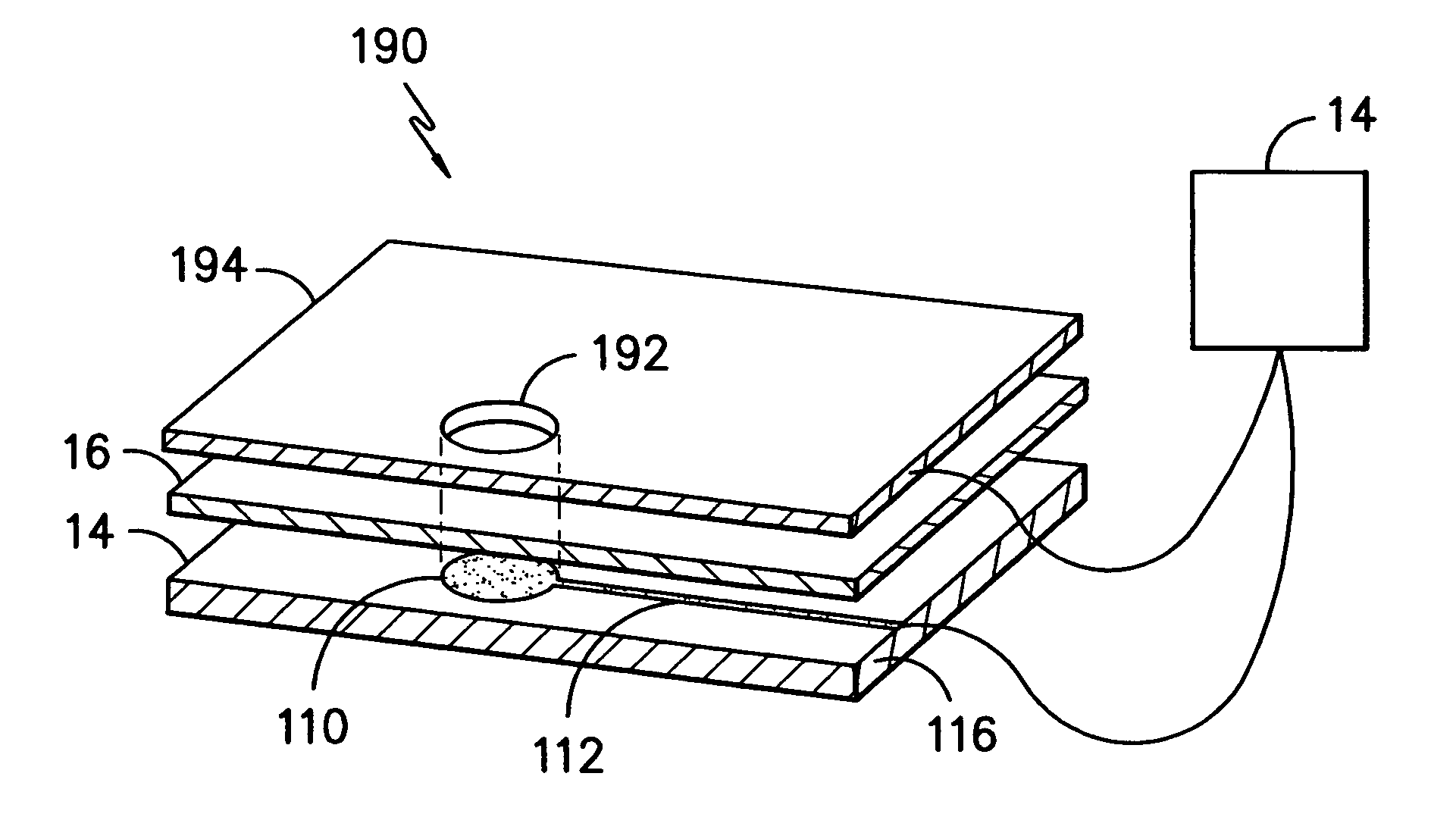
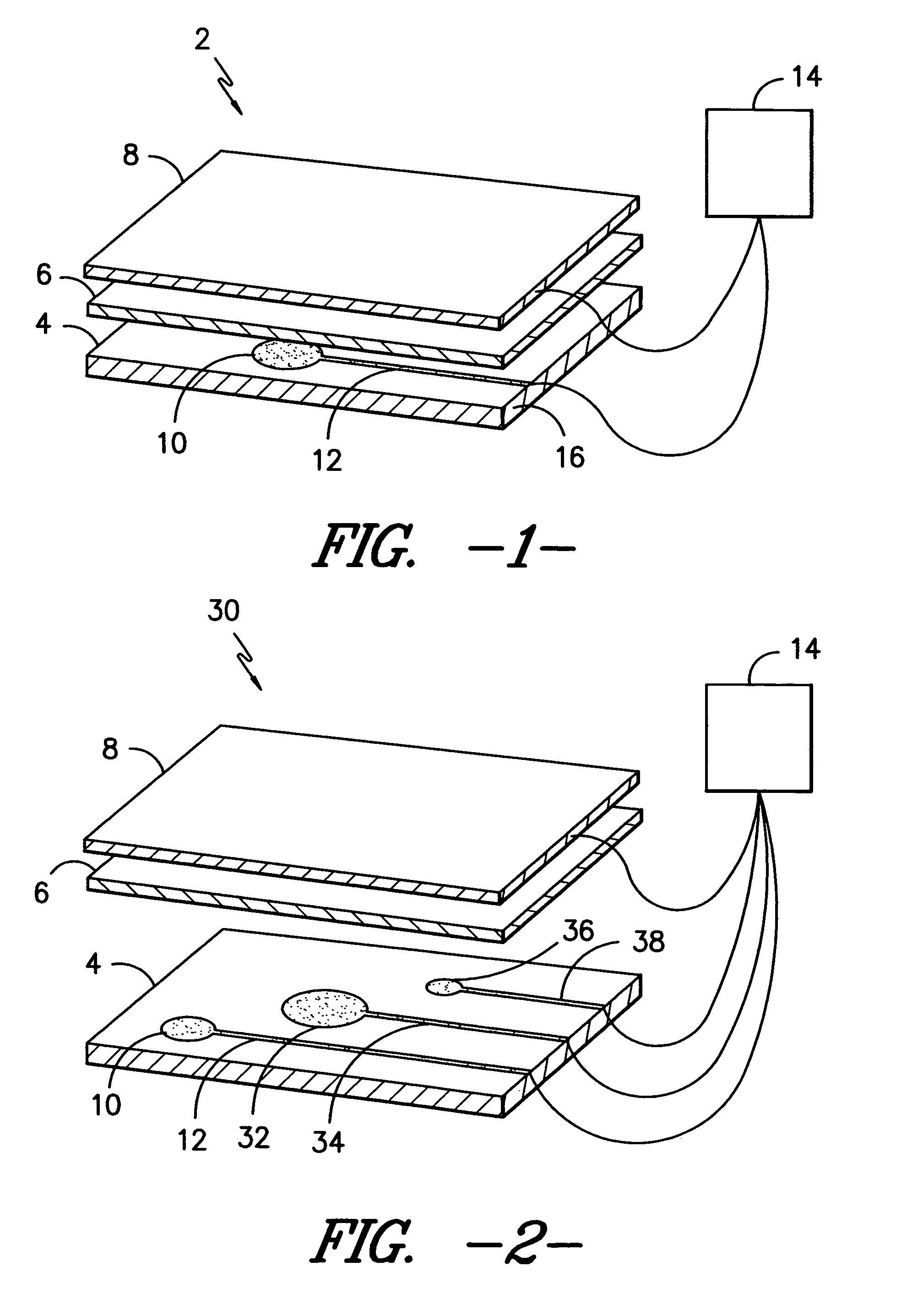
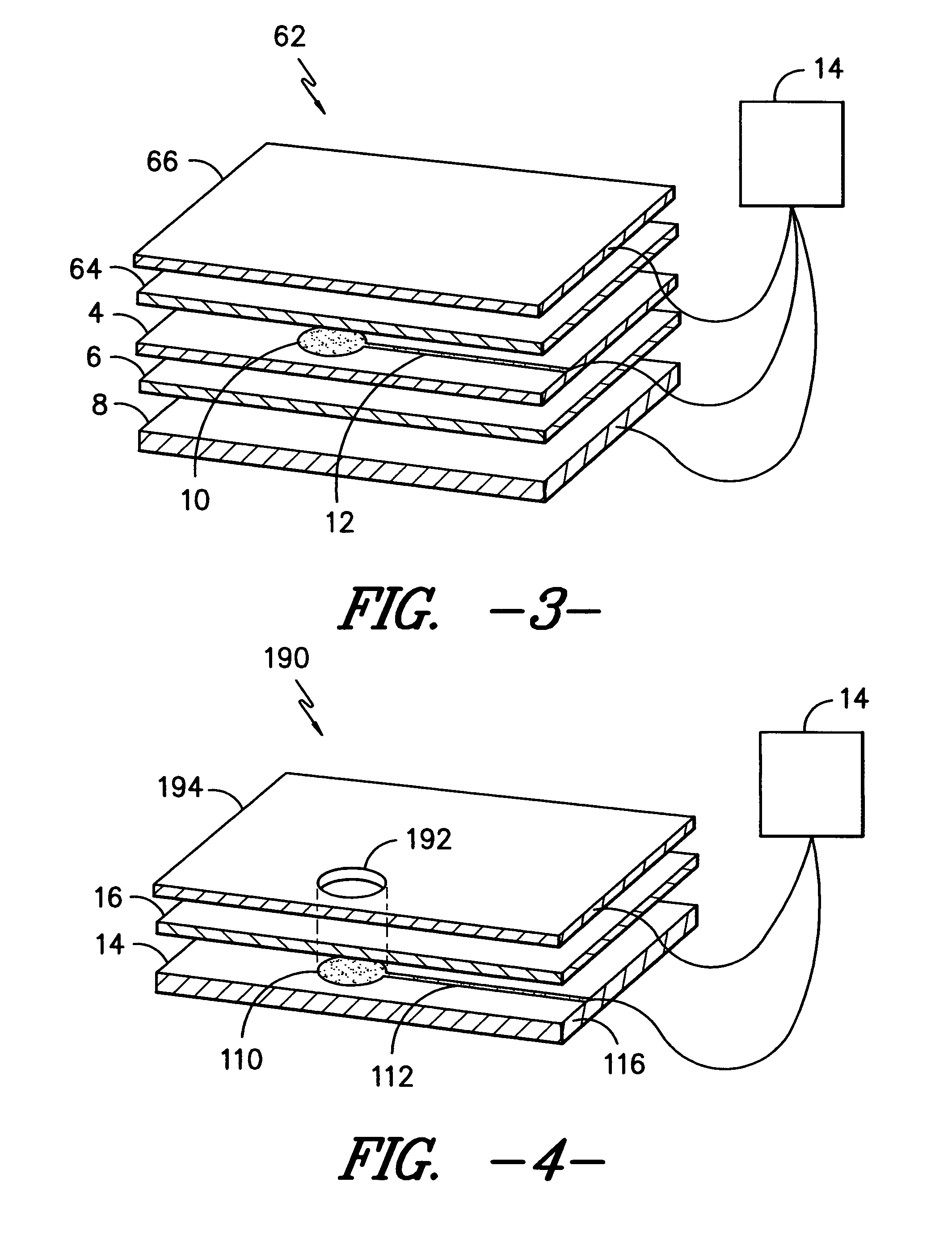
[0011]An important advantage of the present invention is the way the components, namely, the detector-and-trace layer, dielectric layer, conductive reference layer and penetration connector can be assembled to form the present capacitive sensor in a large-scale manufacturing process. Coating, gluing, and screen printing operations can be easily automated. Such operations can make a very large capacitive sensor array or a large fabric from which individual sensors or sensor arrays can be cut.
[0012]Another important feature of the present invention is compatibility with the use of penetration connectors for quickly and easily connecting traces and the reference layer to a capacitance meter (an electrical measurement system) so that electrical signals can be applied or measured from the present sensor without the need for customized electrical connections.
[0013]Still another feature of the present invention is the use of capacitance rather than resistance for sensing contact. Resistance typically requires the two conductive surfaces to touch; capacitance, in some embodiments not only does not require touching but does not even require physical contact with the sensor in some embodiments of the present invention, but mere proximity of a button with the user's finger. Capacitance may also be used to measure the pressure of contact and not just the fact of contact.
[0014]These and other features and their advantages will be apparent to those skilled in the art of electrical circuits and capacitive circuits from a careful reading of the Detailed Description of Preferred Embodiments accompanied by the following drawings.

Problems solved by technology

These systems often require direct contact between the person and the sensing system and may not work, if for example the person is wearing a glove.
Additionally, capacitive coupling may not be well suited to quantitatively measuring the applied pressure or proximity, but are capable of binary (on / off) sensing.
These patents teach the use of flexible conductive and dielectric layers, but they do not teach a system which can be used to determine location, nor do they teach systems with multiple sensors (beyond the simple case of replications of a single sensor).

Method used


Image

  • Printed capacitive sensor
  • Printed capacitive sensor
  • Printed capacitive sensor

Examples


example

Example 1

[0063]A switch panel was made by laminating together multiple layers as shown in FIG. 5. All percentages are by weight unless otherwise specified.

[0064]Two identical resilient structures were made, consisting, in order, of:

[0065]I) a protective layer 104 of 100 g / m2 CelFil 100 spunbonded polyester nonwoven fabric from Polymeross y Derivados of Mexico,

[0066]II) a 1st conductive layer 101 of 100 micron thick Velostat 1704 conductive film from 3M Corporation of St. Paul, Minn., and

[0067]III) a resilient separating layer 102 of 8 mil thick Duraflex PT9300 polyurethane film from Deerfield Urethane of Mass. The 1st conductive layer 101 was used as a ground plane to shield the device from outside interference.

[0068]Next a 2nd conductive layer 108 was made starting with the same nonwoven fabric as in protective layer 104. This was coated with a conductive paste consisting of a mixture of 60% Hycar 26-1199 binder from Noveon of Gastonia N.C., 10% SFG-15 graphite from Timcal of Bodio...

example 2

[0072]A second structure was made, identical to that in Example 1 except that the polymer in the resilient separating layer 102 was replaced with 3 mil thick M823 silicone film from Specialty Silicone Products of Ballston Spa, N.Y.

example 3

[0073]A second structure was made, identical to that in Example 1 except that the polymer in the resilient separating layer 102 was replaced with 44 mil thick T-1505 HypurCEL polyurethane foam from Rubberlite Incorporated of Huntington, W.Va.

[0074]Table A shows the measured capacitances of each of the samples in Examples 1-3. These values are after subtracting out the 44 pF of capacitance between the cables leading from the panels to the multimeter. The pattern of the printed detector and trace elements is shown in FIG. 6. Detectors 120 were connected with the edge of the device buy the long trace 122 and the short trace 121. Also printed were the ground connections 126 and the pin connections 124.

[0075]

TABLE ALong trace (pF) 122Short trace (pF) 121SampleQuiescentPressedQuiescentPressedExample 176843440Example 270834156Example 329391424

[0076]Table A shows that a thinner dielectric will give a larger capacitance, but that a thicker dielectric may give a larger relative change in capa...


PUM

PropertyMeasurementUnit
voltagesaaaaaaaaaa
voltagesaaaaaaaaaa
thicknessaaaaaaaaaa

Abstract

The invention relates to a flexible, resilient capacitive sensor suitable for large-scale manufacturing. The sensor comprises a dielectric, an electrically conductive detector and trace layer on the first side of the dielectric layer comprising a detector and trace, an electrically conductive reference layer on a second side of the dielectric layer, and a capacitance meter electrically connected to the trace and to the conductive reference layer to detect changes in capacitance upon interaction with detector. The sensor is shielded to reduce the effects of outside interference.

Description

TECHNICAL FIELD[0001]This invention relates to a flexible capacitive sensor. More particularly, the invention relates to a capacitive sensor suitable for large-scale manufacturing, that is both physically flexible and flexible in its applications, and that senses incremental changes in pressure based on the changes in the capacitance of the sensor.BACKGROUND[0002]Sensors, as the term is used here, refer to systems that react to a change in the environment. Pressure sensors react to an applied force or pressure using a variety of physical principles. Optical sensors change their optical properties under applied force. Similarly, electrically resistive, or simply resistive, sensors have an electrical resistance that changes under applied force. Piezoresistive sensors measure the change in electrical resistance of a piezoresistive material as pressure is applied.[0003]Capacitive sensors change capacitance. This can be in response to an applied force; it can also be in response to the p...

Claims


Application Information

Patent Timeline
Patent Type & Authority Patents(United States)
IPC IPC(8): G01L1/14G01R27/28
CPCG01D5/2405G01L1/14H03K17/962G01L1/142H03K2217/960755
Inventor DEANGELIS, ALFRED R.WILSON, D. BRUCEMAZZEO, BRIAN A.
Owner MILLIKEN & CO
Why Eureka
Try Eureka