Optical beam transformer module for light coupling between a fiber array and a photonic chip and the method of making the same

a technology of optical beam transformer and fiber array, which is applied in the field of optical beam transformer module for light coupling between a fiber array and a photonic chip and the method of making the same, can solve the problems of large and expensive optical subsystems made from discrete optical components that are interconnected and packaged with fiber pigtails, and the cost of iii–v semiconductor based beam spot size converters, so as to achieve high placement accuracy and low cost

Inactive Publication Date: 2007-12-04
HO SENG TIONG
View PDF69 Cites 51 Cited by
  • Summary
  • Abstract
  • Description
  • Claims
  • Application Information

AI Technical Summary

Benefits of technology

[0014]Embodiments of the present invention provide a device platform to Auto-align photonic chips with other photonic chips, optical components or optical fibers with high placement accuracy. The device platform comprises one or more optical couplers to focus or collimate light from one optical element to another. The devic

Problems solved by technology

Currently, photonic integration is a topic of interest because optical subsystems made from discrete optical components that are interconnected and packaged with fiber pigtails are large and expensive.
However, photonic integration also brings new challenges.
III–V semiconductor based beam spot size converters are expensive, because III–V semiconductor materials such as InP are expensive (as compared to, for example, Si or SiO2).
In addition, this approach cannot be easily extended to the case where multiple input and out

Method used


Image

  • Optical beam transformer module for light coupling between a fiber array and a photonic chip and the method of making the same
  • Optical beam transformer module for light coupling between a fiber array and a photonic chip and the method of making the same
  • Optical beam transformer module for light coupling between a fiber array and a photonic chip and the method of making the same

Examples


Embodiment Construction

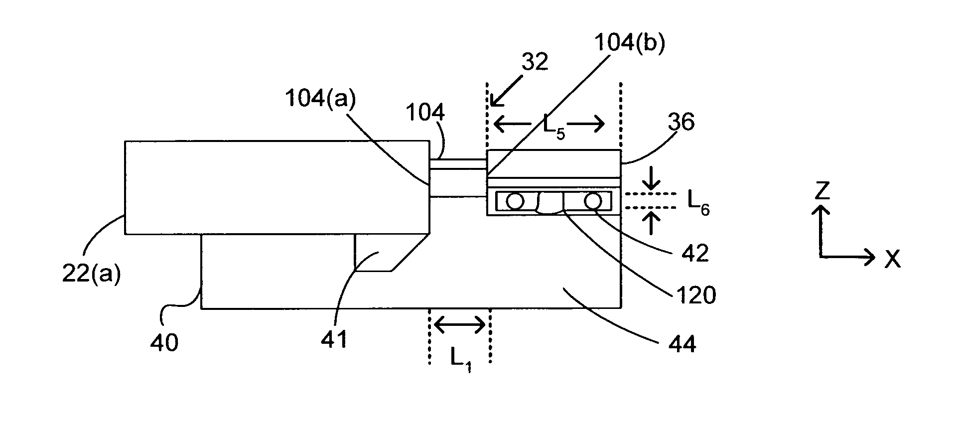
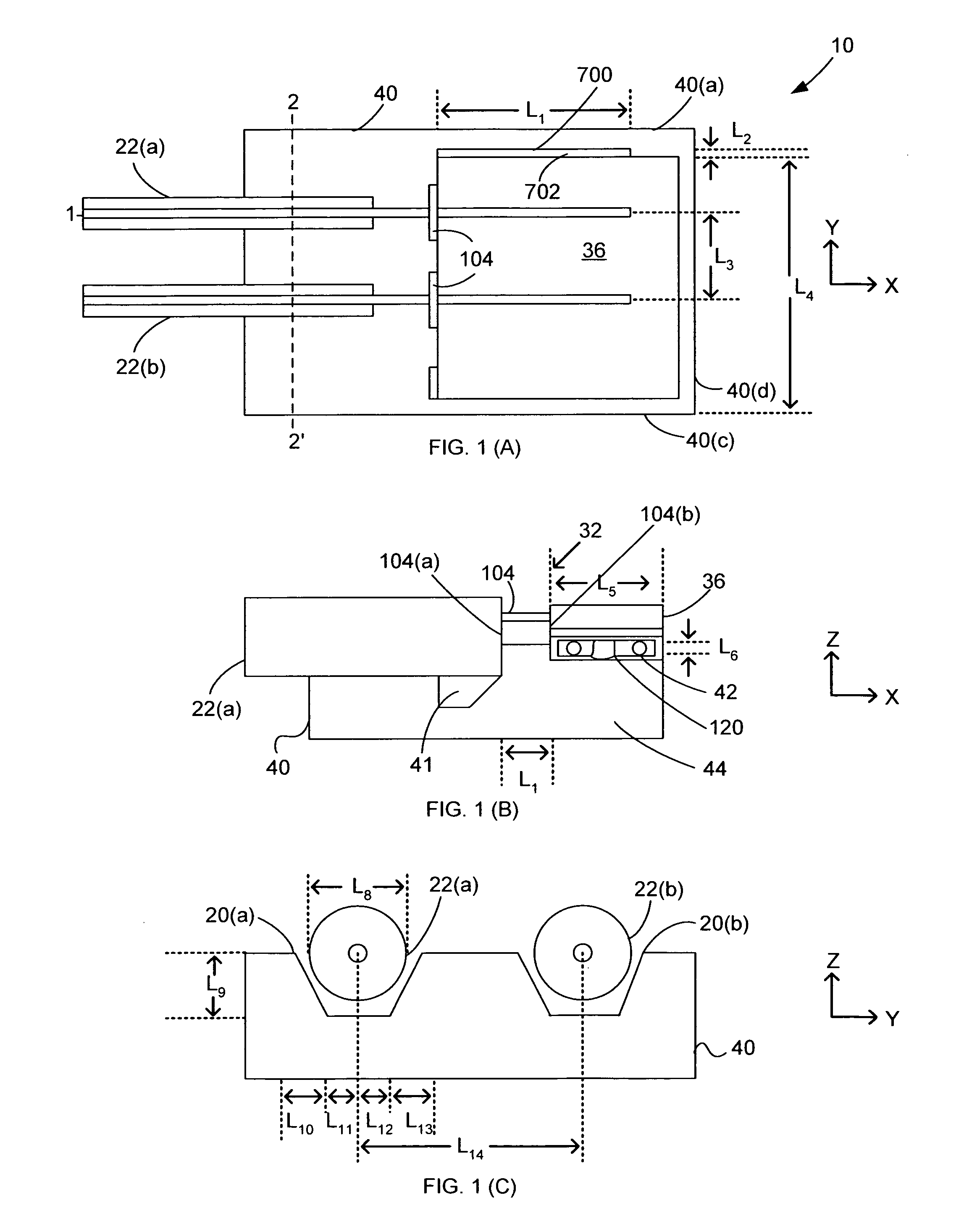
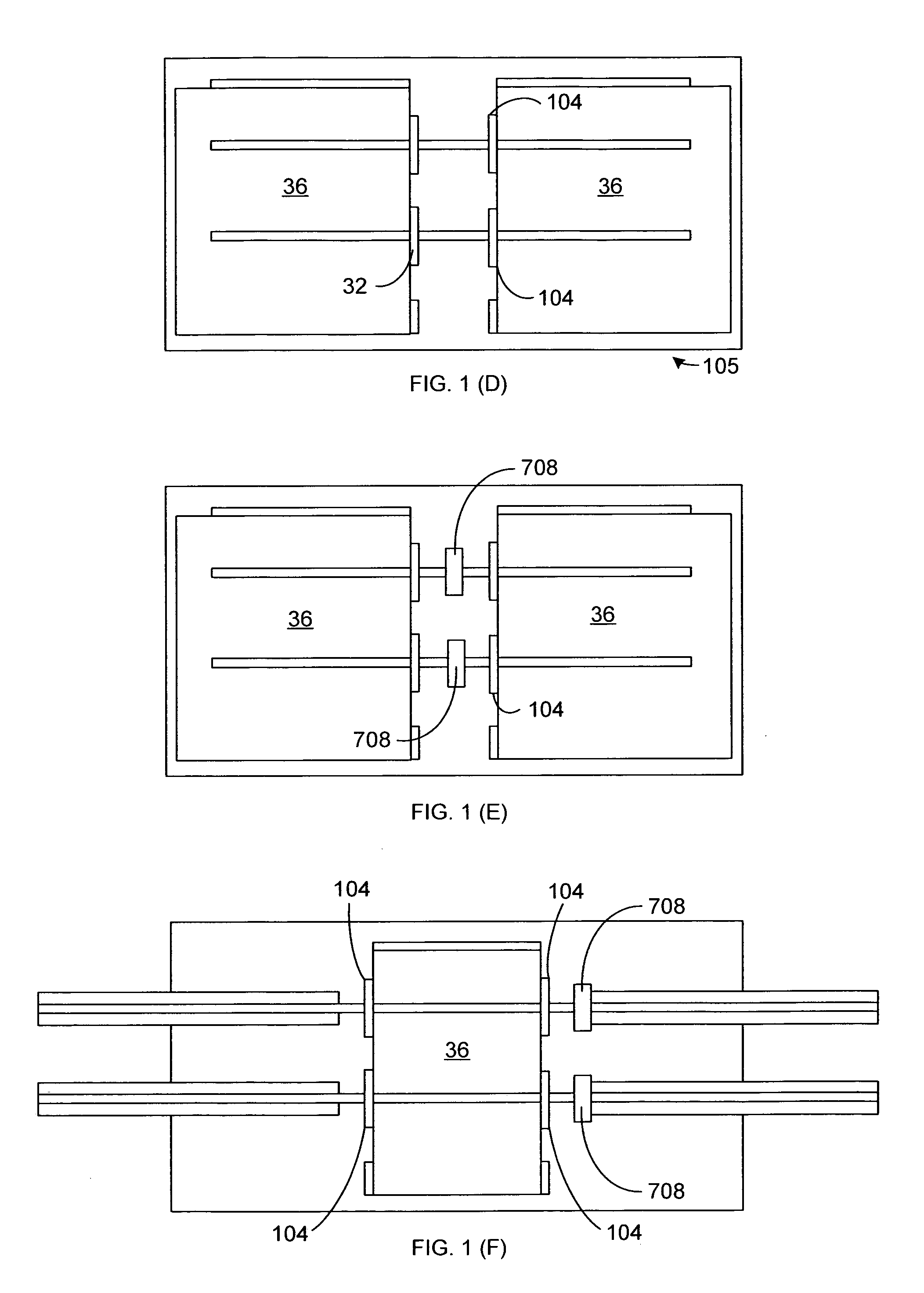
[0054]Embodiments of the present invention provide a device platform to auto-align photonic chips with other photonic chips, optical elements, or optical fibers with high placement accuracy. The device platform comprises one or more optical couplers to focus or collimate light from one optical component to another. One or more inputs and / or outputs from each photonic chip can be in communication with multiple optical elements, optical chips, or fibers. The device fabrication methods described herein are similar to those used in fabricating silicon based planar integrated circuit and hence allows for mass production at low cost. Embodiments of the invention also relate to the processing steps for fabricating an optical coupler together with one or more fiber positioning grooves and a photonic chip pocket. In embodiments of the invention, the alignment of the photonic chip, the coupler, and an optical fiber is easier and more accurate than in conventional processes.

[0055]Described her...


PUM


Abstract

Optical modules and methods for making optical modules are described. In one embodiment, an optical module includes a substrate assembly including a photonic chip mounting region, and a groove extending towards the photonic chip mounting region. A waveguide is disposed within the groove. A plurality of spacers is on the chip mounting region, each spacer having a predetermined height. A photonic chip is placed on the plurality of spacers and above the chip mounting region, and an optical coupler is between the photonic chip and the waveguide.

Description

[0001]This application claims the benefit of the filing date under 35 U.S.C. § 119(e) of Provisional U.S. Patent Application Ser. No. 60 / 406,723, filed on Aug. 28, 2002, which is hereby incorporated by reference in its entirety.CROSS REFERENCES TO RELATED APPLICATIONS[0002]This application is related to co-pending U.S. patent application Ser. No. 10 / 056,430, entitled “Connection of a Waveguide Fiber Coupler with an Optical Fiber and a Photonic Integrated Chip,” filed Oct. 22, 2001.[0003]This application is also related to co-pending U.S. patent application Ser. No. 10 / 083,674, entitled “Integrated Planar Composite Coupling Structures for Bi directional Light Beam Transformation Between a Small Mode Size Waveguide and a Large Mode Size Waveguide,” filed Oct. 22, 2001.[0004]This application is also related to co-pending U.S. patent application Ser. No. 10 / 310,330, entitled “Connection Between a Waveguide Array and a Fiber Array,” filed Dec. 4, 2002.[0005]This application is also relat...

Claims


Application Information

Patent Timeline
IPC IPC(8): G02B6/42H04B10/12G02B6/136G02B6/36
CPCG02B6/136G02B6/3636G02B6/3692G02B6/423G02B6/4232G02B6/3652
Inventor ZHOU, YANCHENG, SHIDEHO, SENG-TIONG
Owner HO SENG TIONG
Why Eureka
Try Eureka