Laser micromachining method

a laser and micro-machining technology, applied in the field of micro-machining, can solve the problems of reducing the fluence and ablation capability of the laser, the inability of conventional lasers (traditionally focused lasers with long pulse duration, such as nanosecond lasers) to produce high-quality cuts through semiconductor wafers, and the inability of lasers to integrate laser technology for die singulation

Inactive Publication Date: 2007-12-04
INTEL CORP
View PDF4 Cites 42 Cited by
  • Summary
  • Abstract
  • Description
  • Claims
  • Application Information

AI Technical Summary

Problems solved by technology

Next generation semiconductor devices, however, will use new materials, such as low dielectric constant (low-k) interlayer dielectric layers (ILDs) that may be incapable of withstanding the sheer forces exerted during the wafer sawing process.
However, the integration of laser technology to perform die singulation is not without its challenges.
Conventional lasers (traditionally focused lasers having long pulse durations, such as nanosecond lasers) are currently incapable of producing high-quality cuts through a semiconductor wafer.
This is because the laser's fluence is not intense enough to ablate completely through the entire thickness of the wafer.
Loosening the laser's focus geometry to increase the laser's depth-of-focus does not solve the problem because enlarging the laser's depth-of-focus also reduces the laser's fluence and ablation capabilities.
Conventional focusing does not improve dicing / milling capabilities because even tight focusing cannot produce the amount of fluence needed to ablate entirely through the thickness of the substrate.
Increasing overall laser power to compensate for this limitation generates heat and compromises the quality of the laser cut.
Heat produces thermal effects and mechanical damage.
Both of which can impact a semiconductor device performance and yield.
A disadvantage of using this approach is that two different processes must be combined to singulate the wafer.
The combination is more complicated, costly, and slower than using a single laser or sawing process.
Major disadvantages of this process include its low throughput (low number of wafers-per-hour) and inaccurate laser beam placement (10 microns or more beam pointing instability).
Unless process throughputs can be increased, this approach will probably not be considered a viable dicing alternative by high volume semiconductor manufacturers.
Disadvantages of using this process include the physical force of the water jet and the water cavitation pressure wave that forms in the trench during processing.
Both of which can result in increased defect densities as well as delamination and cracking of layers formed on the wafer.

Method used


Image

  • Laser micromachining method
  • Laser micromachining method

Examples


Embodiment Construction

[0010]In the following detailed description, a method for laser micromachining is disclosed. Reference is made to the accompanying drawings within which are shown, by way of illustration, specific embodiments by which the present invention may be practiced. It is to be understood that other embodiments may exist and that other structural changes may be made without departing from the scope and spirit of the present invention.

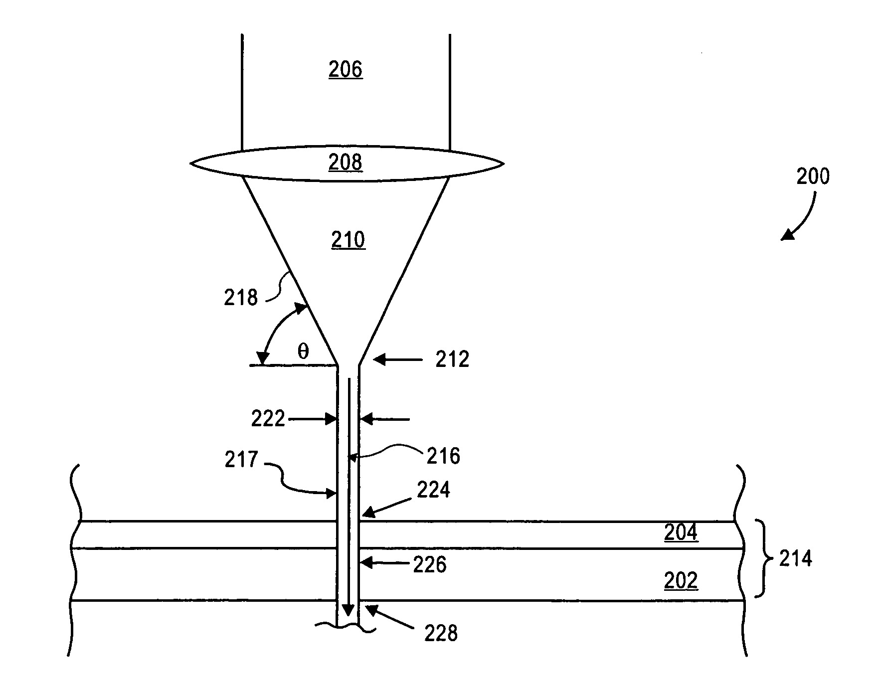
[0011]Using embodiments of the present invention, collimated beams, incident to converging beam geometry pulses from an ultrafast laser, can be used to scribe, dice, or mill a workpiece. The collimated beam can maintain a uniform diameter and high intensity optical energy while ablating through the entire thickness of the workpiece. In one embodiment, the workpiece is a semiconductor wafer. Embodiments of the present invention overcome depth-of-focus problems encountered with conventional lasers. And, because ablation is the result of using a short pulse duratio...


PUM

PropertyMeasurementUnit
pulse energyaaaaaaaaaa
diameteraaaaaaaaaa
ionization energyaaaaaaaaaa

Abstract

A laser micromachining method is disclosed wherein a workpiece is milled using an incident beam from a laser beam focused above the surface of the workpiece. The incident beam is guided by a plasma channel generated by the incident beam. The plasma channel, which has a relatively constant diameter over an extended distance, is generated by continual Kerr effect self-focusing balanced by ionization of air beam defocusing.

Description

FIELD OF THE INVENTION[0001]Embodiments of the present invention relate generally to micromachining and more specifically to laser micromachining of semiconductor substrates.BACKGROUND OF THE INVENTION[0002]Conventional semiconductor wafer singulation is done using mechanical dicing saws. Next generation semiconductor devices, however, will use new materials, such as low dielectric constant (low-k) interlayer dielectric layers (ILDs) that may be incapable of withstanding the sheer forces exerted during the wafer sawing process. Lasers, either alone or in combination with saws, are being considered as alternatives to conventional sawing. However, the integration of laser technology to perform die singulation is not without its challenges.[0003]Conventional lasers (traditionally focused lasers having long pulse durations, such as nanosecond lasers) are currently incapable of producing high-quality cuts through a semiconductor wafer. This is because the laser's fluence is not intense e...

Claims


Application Information

Patent Timeline
Patent Type & Authority Patents(United States)
IPC IPC(8): H01L21/00
CPCB23K26/0635B23K26/4075B23K2201/40B23K26/0624B23K26/40B23K2101/40B23K2103/50
Inventor VORONOV, SERGEI L.RUMER, CHRISTOPHER L.
Owner INTEL CORP
Why Eureka
Try Eureka