Patterning using wax printing and lift off

a technology of liftoff and wax printing, applied in the field of patterning process, can solve the problems of increasing the size and complexity of tft arrays, the need for large display areas, and the inability to manufacture these devices using conventional semiconductor processes, so as to reduce the cost of production, simplify the alignment of liftoff patterns, and improve the effect of accuracy

Inactive Publication Date: 2007-12-18
PALO ALTO RES CENT INC
View PDF5 Cites 20 Cited by
  • Summary
  • Abstract
  • Description
  • Claims
  • Application Information

AI Technical Summary

Benefits of technology

[0012]The invention is directed towards printing systems and methods that can perform liftoff processing by using printed liftoff patterns. By printing the liftoff pattern, the complex photolithography steps can be eliminated from the liftoff process, thereby reducing production costs and simplifying the patterning process.
[0014]Because a printing operation for a liftoff pattern is much less sensitive to environmental factors, the use of a printed liftoff pattern beneficially allows the liftoff process to be carried out in a lab environment, rather than in a cleanroom, which further reduces the cost of production. In addition, a liftoff pattern can be printed on non-planar surfaces, unlike photolithography, which requires a very flat surface to maintain pattern fidelity.
[0015]The printing of a liftoff pattern also simplifies the alignment of that liftoff pattern with underlying elements, since photomask handling is eliminated completely. This is particularly beneficial when creating low coverage liftoff patterns (i.e., liftoff patterns that only affect a small portion of the overall patterned area, such as via masks), since the photomasks required for such low coverage patterns are mostly opaque, and are therefore difficult to align with underlying elements.
[0016]According to another embodiment of the invention, a liftoff pattern can be created by printing multiple layers for some or all of the elements making up the liftoff pattern. Due to the scalloped sidewall profile of those multi-layer elements, a liftoff operation using the printed liftoff pattern will create apertures in the patterned liftoff layer that exhibit a diverging profile (i.e., the width of the aperture increases with depth). The patterned liftoff layer can then be used as an etch mask for an underlying layer. Because of the diverging profile of the apertures in the patterned liftoff layer, the etched portions of the underlying layer will exhibit a converging profile (i.e., the width of the etched aperture decreases with depth). The converging etched aperture profiles beneficially minimize void formation during a subsequent fill operation (e.g., via plug or trench fill).
[0017]According to another embodiment of the invention, the liftoff pattern layout can be separated into discrete design layers having only parallel layout features, and the printed liftoff pattern can be formed by a series of printing operations, wherein the print direction of each printing operation is aligned with the parallel layout features of the design layer being printed. In this manner, the printing of multi-pass features can be avoided, and homogenous, smooth-edged printed patterns can be printed.
[0018]According to another embodiment of the invention, a printed liftoff pattern can be aligned with existing elements in the base layer (and any underlying layers) through the use of alignment marks on the base layer. By calibrating the liftoff pattern printing system against those alignment marks prior to printing the liftoff pattern, alignment between the liftoff pattern and elements on other layers (and within the liftoff pattern itself if the liftoff pattern is separated into different design layers) can be maintained.

Problems solved by technology

In addition, the need for large display areas complicates the fabrication of these devices using conventional semiconductor processes.
In combination, these factors result in ever-increasing TFT array size and complexity.
This is not only due to the demanding nature of the photolithography process itself, but also due to the time and costs involved in producing the delicate photomasks used in the photolithography process.

Method used


Image

  • Patterning using wax printing and lift off
  • Patterning using wax printing and lift off
  • Patterning using wax printing and lift off

Examples


Embodiment Construction

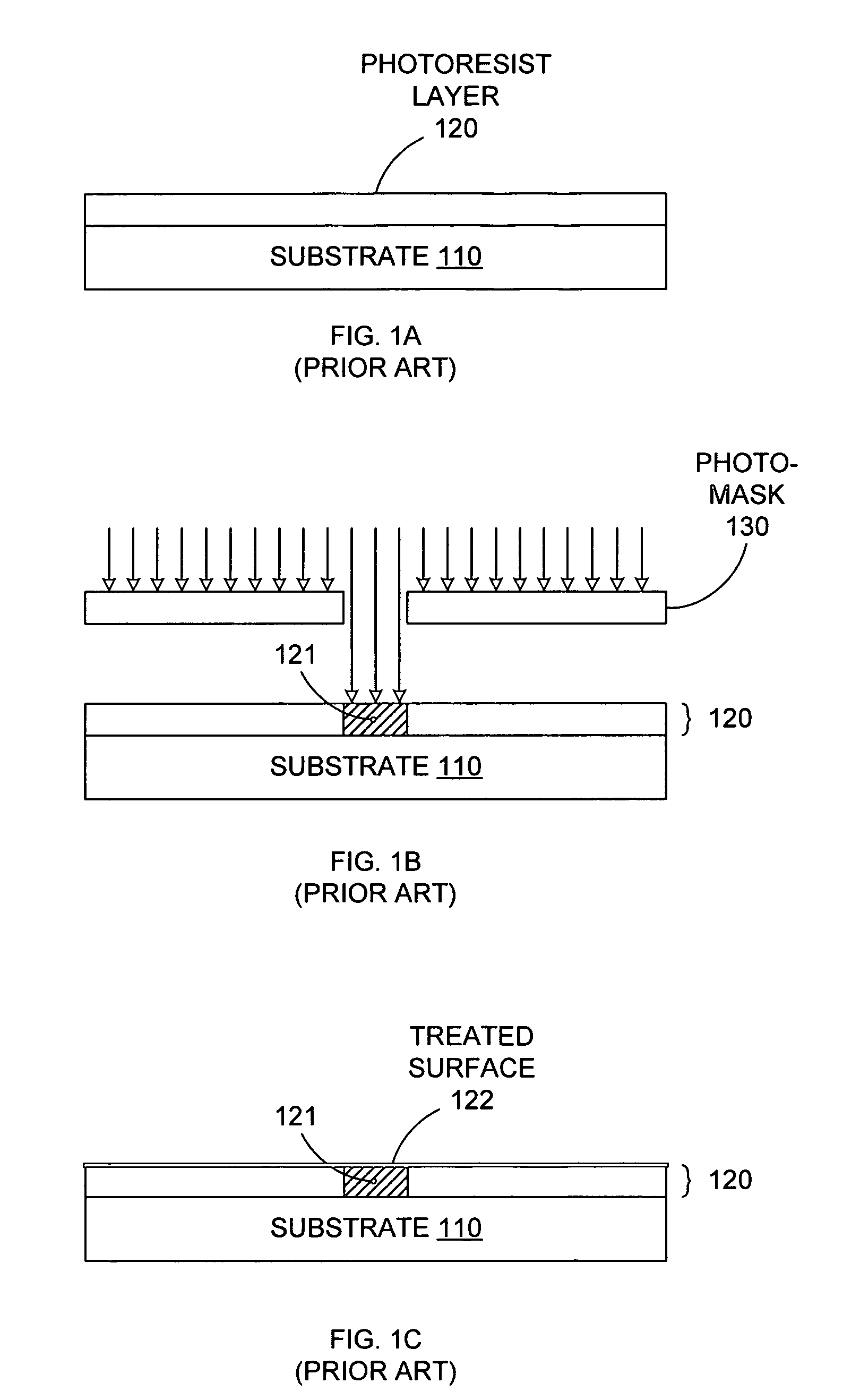
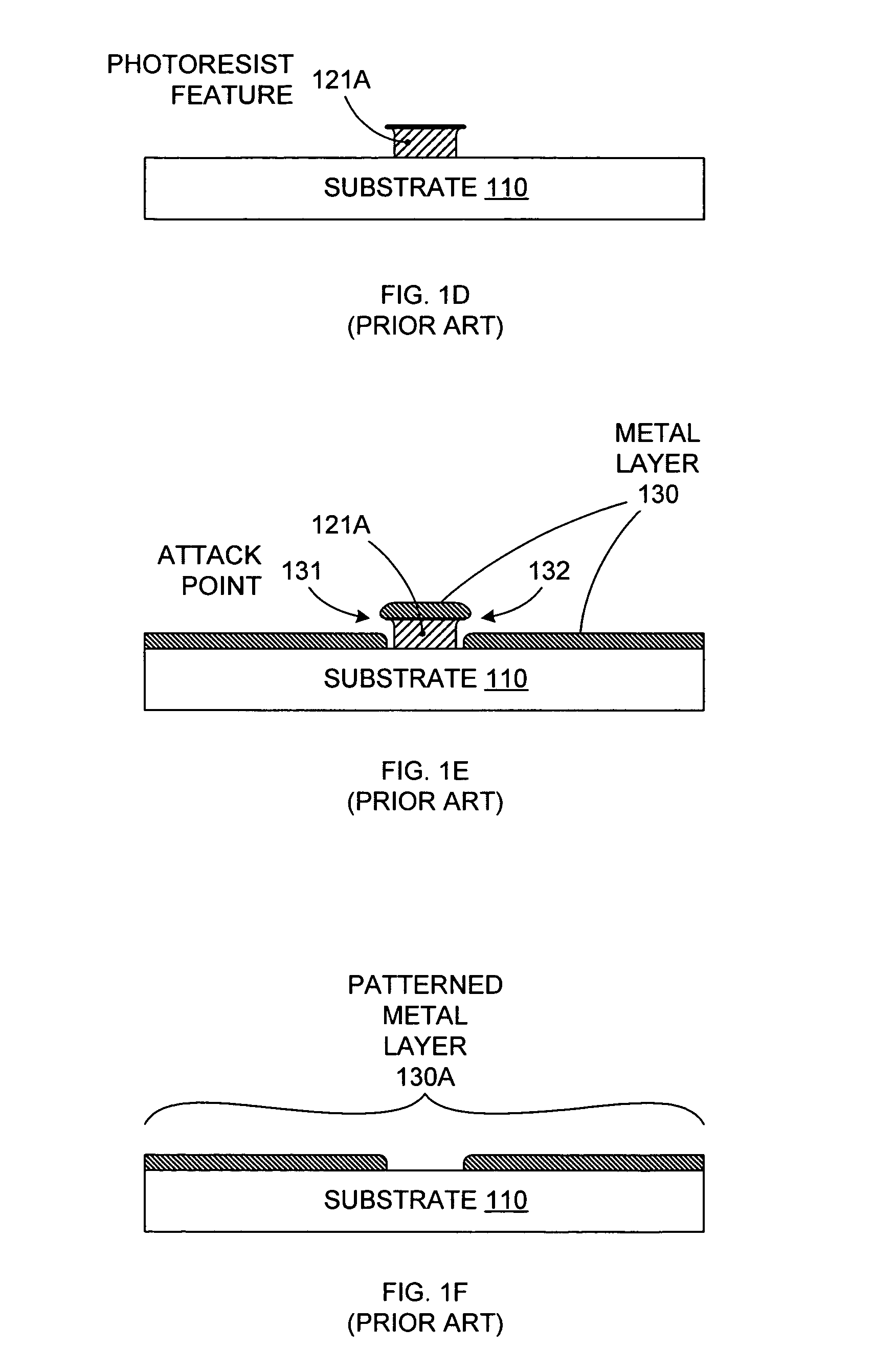
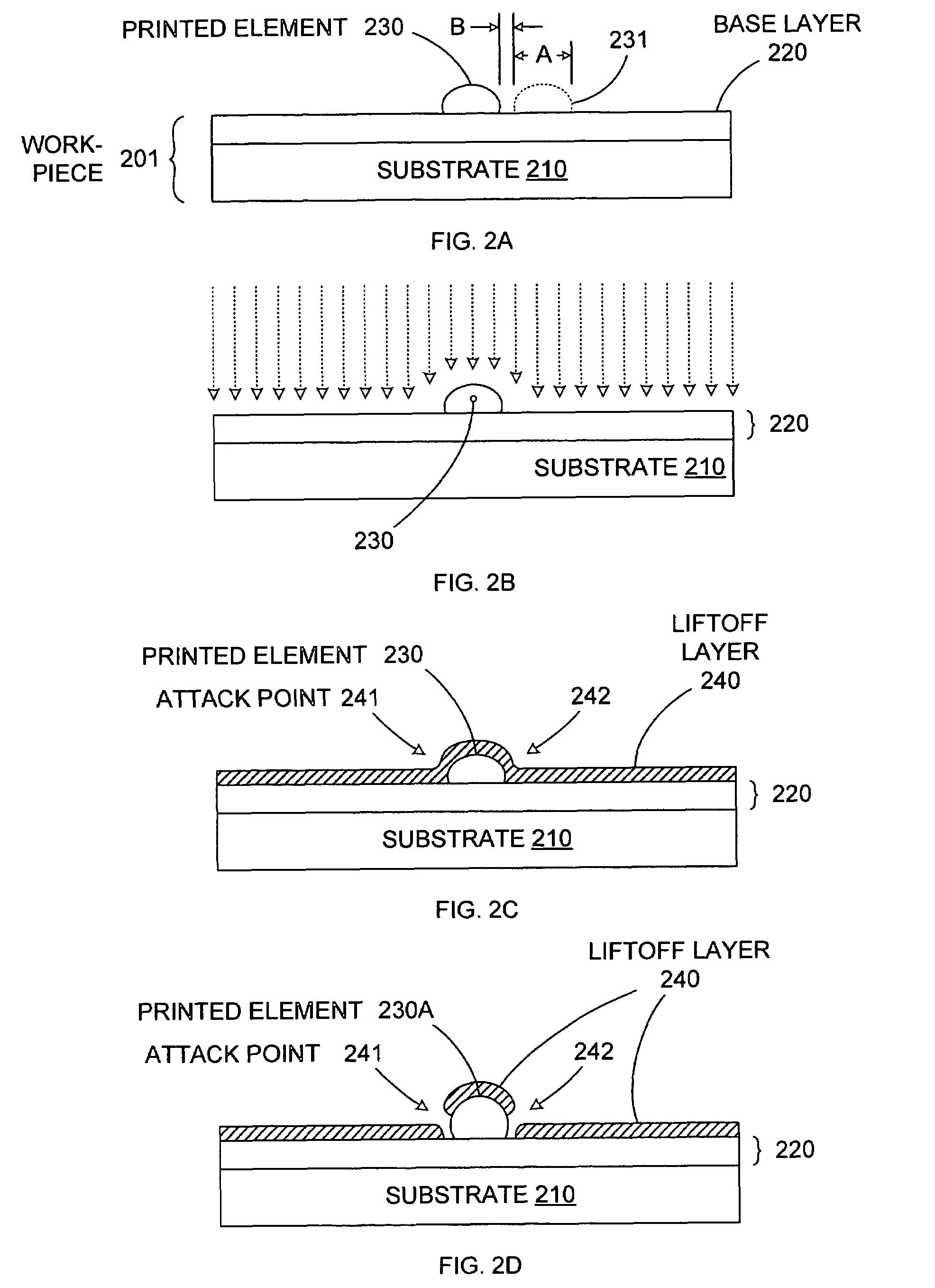
[0033]Printing of integrated circuit (IC) patterns is an emerging technology that attempts to reduce the costs associated with IC production by printing an IC pattern directly on a substrate rather than creating the pattern using the delicate and time-consuming photolithography processes used in conventional IC manufacturing. As described in co-owned, co-pending U.S. patent application Ser. No. [XC-030], the printed IC pattern typically comprises actual IC features (i.e., elements that will be incorporated into the final IC, such as the gates and source and drain regions of thin film transistors, signal lines, opto-electronic device components, etc.) or a mask for subsequent semiconductor processing (e.g., etch, implant, etc.).

[0034]The invention adapts pattern printing to create a liftoff pattern for use in a liftoff process, thereby providing an alternative to the costly and sensitive photolithography operations used in conventional liftoff processes. According to various embodime...


PUM

PropertyMeasurementUnit
structurally homogenousaaaaaaaaaa
angle of rotationaaaaaaaaaa
angleaaaaaaaaaa

Abstract

A method for performing a liftoff operation involves printing a liftoff pattern using low-resolution patterning techniques to form fine feature patterns. The resulting feature size is defined by the spacing between printed patterns rather than the printed pattern size. By controlling the cross-sectional profile of the printed liftoff pattern, mask structures may be formed from the liftoff operation having beneficial etch-mask aperture profiles. For example, a multi-layer printed liftoff pattern can be used to create converging aperture profiles in a patterned layer. The patterned layer can then be used as an etch mask, where the converging aperture profiles result in desirable diverging etched features.

Description

[0001]This invention was made with Government support under 70NANBOH3033 awarded by NIST / ATP. The Government has certain rights in this invention.BACKGROUND OF THE INVENTION[0002]1. Field of the Invention[0003]Further, the invention relates generally to electronic materials processing, and more particularly to a system and method for performing a patterning process without using photolithography.[0004]2. Related Art[0005]Modern video and computer LCD (liquid crystal display) displays typically include large arrays of thin film transistors (TFTs) for addressing the individual pixels in the displays. As the demand for larger LCD displays continues to rise, the TFT arrays used in those LCD displays must include increasing numbers of TFTs and more complex interconnect structures. In addition, the need for large display areas complicates the fabrication of these devices using conventional semiconductor processes. In combination, these factors result in ever-increasing TFT array size and ...

Claims


Application Information

Patent Timeline
Patent Type & Authority Patents(United States)
IPC IPC(8): G03C5/00G03F7/00H01L21/28H01L21/027H01L21/033H01L21/306H01L21/311H01L21/336H01L21/768H01L29/786
CPCH01L21/76802H01L21/31144H01L21/0335H01L21/0272
Inventor PAUL, KATERI E.WONG, WILLIAM S.READY, STEVEN E.LUJAN, RENE A.
Owner PALO ALTO RES CENT INC
Why Eureka
Try Eureka