

Dielectric ceramic composition, electronic device and production methods of the same
a technology of dielectric ceramics and electronic devices, applied in ceramics, fixed capacitors, natural mineral layered products, etc., can solve the problems of unreliable insulation resistance and difficult to reduce the achieve low defect rate of insulation resistance, accelerated lifetime of insulation resistance is long, and the frequency dependency is small
- Summary
- Abstract
- Description
- Claims
- Application Information
AI Technical Summary
Benefits of technology
Problems solved by technology
Method used
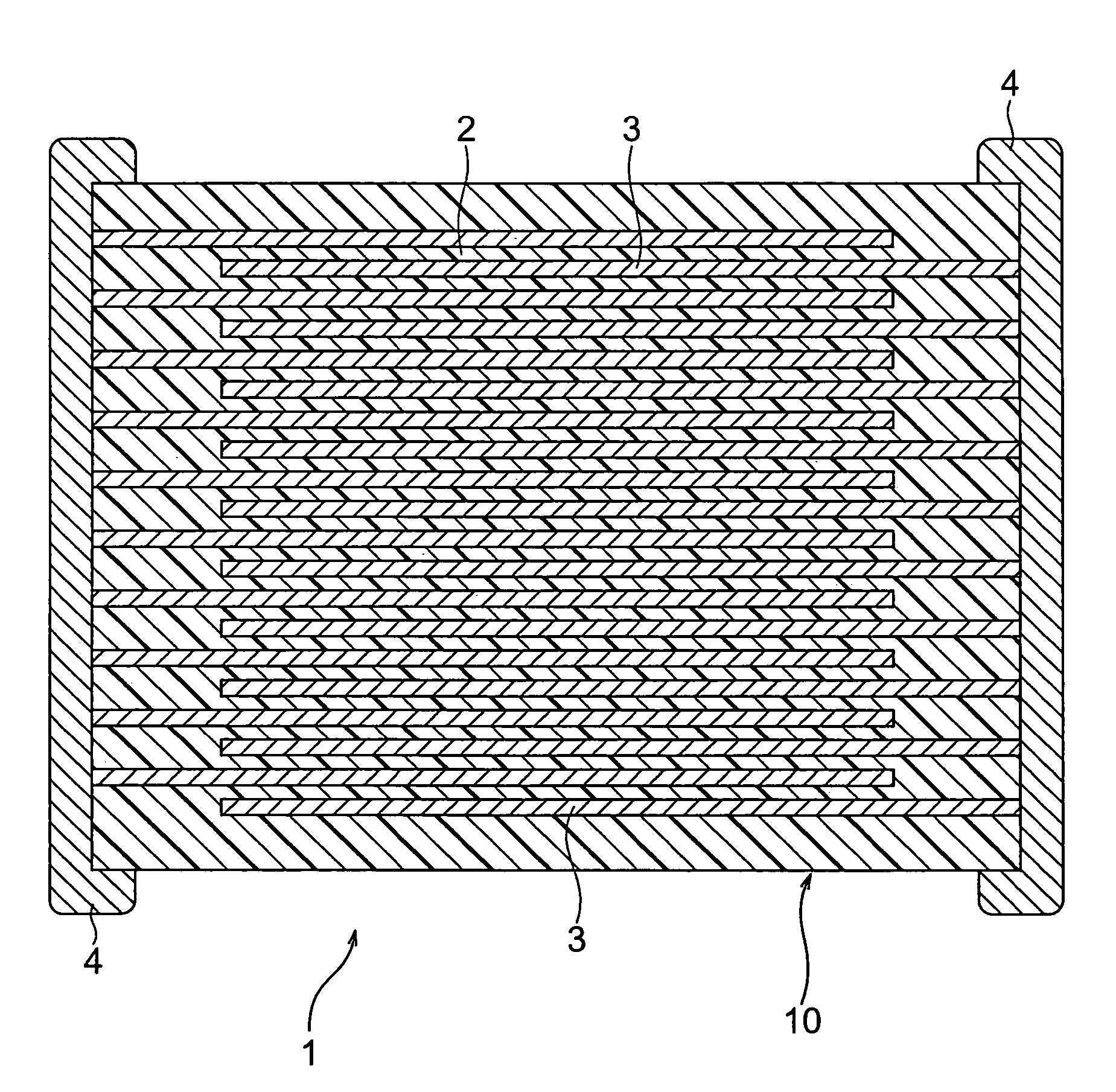
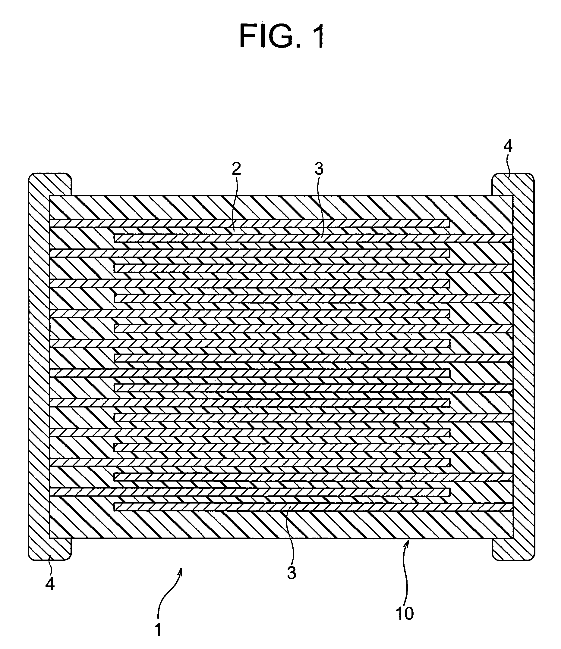
Image

Examples
example 1
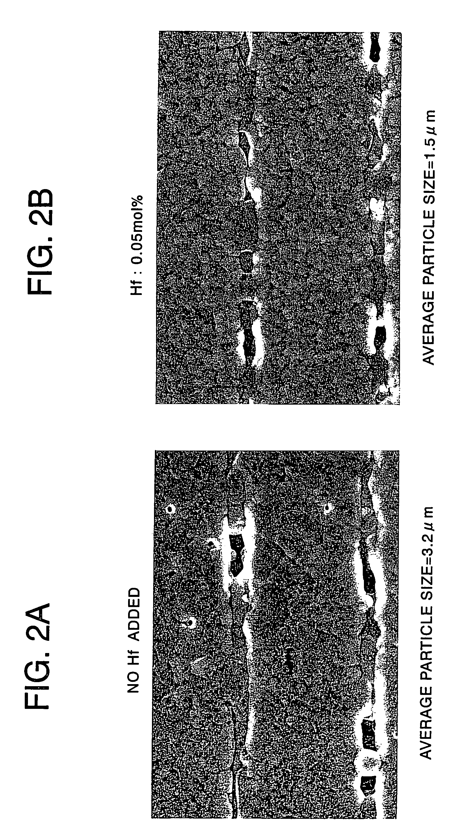
[0136]First, as starting materials for producing a dielectric material, main component materials (SrCO3, CaCO3, TiO2, ZrO2 and HfO2) and subcomponent materials (including a glass component) each having an average particle diameter of 0.1 to 1.5 μm were prepared. As the subcomponent materials, carbonate (MnO3 and BaCO3) or oxides (Al2O3, SiO2 and Y2O3, etc.) were used.
[0137]After weighing the materials, so that a composition after firing would be the composition shown in Table 1 below, water as a medium was added to the materials and mixed by a ball mill for 16 to 40 hours to perform high dispersion mixing. After that, the mixture was dried, then, calcinated under a condition of 1100 to 1300° C. for 2 to 4 hours. Thus obtained calcinated substance was subjected to wet grinding by a ball mill and dried.
[0138]With 100 parts by weight of the thus obtained dried dielectric material, 4.8 parts by weight of an acrylic resin, 40 parts by weight of methylene chloride, 20 parts by weight of e...
example 2
[0169]Other than weighing the materials, so that a composition after firing would be the composition shown in Table 3 below, capacitor samples were produced in the same way as in the example 1 and the same evaluation was made as that in the example 1. The results are shown in Table 4.
[0170]
TABLE 3Subcomponent 1Subcomponent 2mol % withmol % with respectMain Componentrespect toGlass Componentto 100 mol ofMole Ratios100 mol[(BavCa1−v)O]wSiO2AddingMain ComponentSamplein [(CaxSr1−x)O]m[(TiyZr1−y−zHfz)O2]of Main ComponentMole RatiosQuantityAddingNo.x1 − xy1 − y − zzmMnOAl2O3v1 − vwmol %AdditiveQuantity260.70.30.050.90.05110.50113——270.70.30.050.90.05110.50.10.913——280.70.30.050.90.05110.51013——※290.70.30.050.90.05110.50.50.50.43——300.70.30.050.90.05110.50.50.50.53——310.70.30.050.90.05110.50.50.543——※320.70.30.050.90.05110.50.50.54.13——※330.70.30.050.90.05110.50.50.510.4——340.70.30.050.90.05110.50.50.510.5——350.70.30.050.90.05110.50.50.5115——※360.70.30.050.90.05110.50.50.5116——
[0171]
TABLE ...
example 3
[0176]Other than weighing the materials, so that a composition after firing would be the composition shown in Table 5 below, capacitor samples were produced in the same way as in the example 1, and the same evaluation was made as that in the example 1. The results are shown in Table 6.
[0177]
TABLE 5Subcomponent 1Subcomponent 2mol % withmol % with respectMain Componentrespect toGlass Componentto 100 mol ofMole Ratios100 mol[(BavCa1−v)O]wSiO2AddingMain ComponentSamplein [(CaxSr1−x)O]m[(TiyZr1−y−zHfz)O2]of Main ComponentMole RatiosQuantityAddingNo.x1 − xy1 − y − zzmMnOAl2O3v1 − vwmol %AdditiveQuantity※370.70.30.050.90.05110.50.50.413Mg0.01380.70.30.050.90.05110.50.50.413Mg0.02390.70.30.050.90.05110.50.50.413Mg0.5400.70.30.050.90.05110.50.50.413Mg1.5※410.70.30.050.90.05110.50.50.413Mg2420.70.30.050.90.05110.50.50.413Sc0.5430.70.30.050.90.05110.50.50.413Y0.5440.70.30.050.90.05110.50.50.413La0.5450.70.30.050.90.05110.50.50.413Ce0.5460.70.30.050.90.05110.50.50.413Pr0.5470.70.30.050.90.05110...
PUM
| Property | Measurement | Unit |
|---|---|---|
| particle diameter | aaaaa | aaaaa |
| thickness | aaaaa | aaaaa |
| insulation resistance | aaaaa | aaaaa |
Abstract
Description
Claims
Application Information