Display device and electronic device using the same

a technology of electronic devices and display devices, applied in the field of display devices, can solve the problems of relative hardness of grain boundaries, and achieve the effects of improving the crystallinity of a portion, superior crystallinity, and progressing effective crystallization

Inactive Publication Date: 2007-12-25
SEMICON ENERGY LAB CO LTD
View PDF100 Cites 36 Cited by
  • Summary
  • Abstract
  • Description
  • Claims
  • Application Information

AI Technical Summary

Benefits of technology

[0056]The present invention has been made in view of the above problems. An object of the present invention is to prevent a grain boundary from forming in a channel formation region of a TFT to reduce a deterioration and a variation in characteristics of the TFT such as a reduction in mobility, a rise in threshold value, and an increase in off current so that a display quality of a display device is improved. The present invention can be widely used for not only a display device using an OLED but also a display device using inorganic EL, an FED display device, an electrophoretic display device, a liquid crystal display device, and the like.
[0060]According to the present invention, after the crystallization by laser light, the edges and vicinities of the depression of the semiconductor film or the edges and vicinities of the projection thereof are removed by patterning, and a portion which is located in the central portion and vicinities of the projection and has superior crystallinity is actively used as the active layer of a TFT, in particular, the channel formation region thereof. Thus, it can be prevented that the grain boundaries are formed in the channel formation region of the TFT so that a deterioration of TFT characteristics or an increase in a variation thereof which results from the existence of grain boundaries can be prevented. Note that a range corresponding to the edges and vicinities to be removed can be determined as appropriate by a designer.
[0063]According to the present invention, a mask of the active region (island) of a TFT is laid out, and a shape of the depression or the projection of the insulating film or a position of the edges thereof is designed corresponding to the layout of the island so as to improve the crystallinity of a portion which becomes the island. More specifically, the shape and the size are determined such that the edges of the depression or the projection are not overlapped with the island. Using the insulating film designed according to the layout of the island, a semiconductor film in which grain boundaries are produced near the edges is intentionally formed. A portion which is located near the edges of the semiconductor film and in which a large number of grain boundaries exist is removed by patterning and a portion with relatively superior crystallinity is used as the island. Thus, the technique disclosed according to the present invention is the same as the above mentioned known technique with respect to a point that the semiconductor film is provided on the insulating film with the steps and then crystallized. However, the conventional technique does not include the concept in which the positions of grain boundaries are controlled by using the steps. Accordingly, the present invention is different from the conventional technique. In addition, according to the above papers, a circular beam spot of a laser is used. According to the present invention, a linear laser beam is used so that very effective crystallization can be progressed.

Problems solved by technology

Thus, it is relatively hard to form grain boundaries.

Method used


Image

  • Display device and electronic device using the same
  • Display device and electronic device using the same
  • Display device and electronic device using the same

Examples


embodiment 1

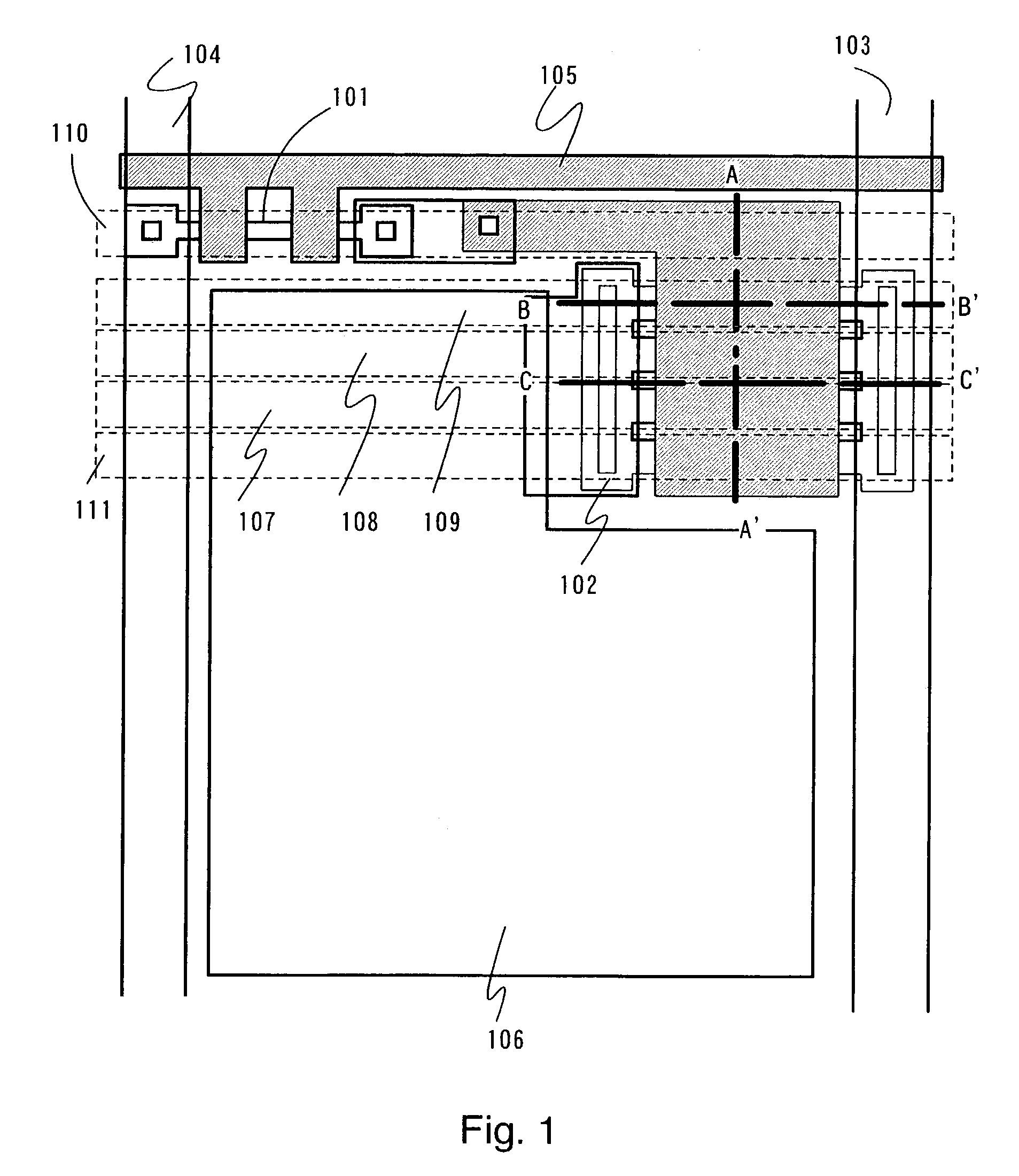
[0091]FIG. 1 shows an example in the case where the present invention is applied to an OLED display device. FIG. 1 is a plan view of TFTs composing a pixel. Here, reference numeral 101 denotes a switching TFT, 102 denotes a driver TFT, 103 denotes a power supply line, 104 denotes a source signal line, and 105 denotes a gate signal line. As described in “Description of the Related Art”, it is important to reduce a variation in driver TFT for driving an OLED in the OLED display device. Thus, in this embodiment, not only a TFT is formed on a depression or a projection of an insulating film having unevenness but also multi-channelization is achieved so that a flow of current is uniformed to suppress a variation in current. A structure of the driver TFT is as follows.

[0092]FIG. 1 shows an example in which the channel of the TFT is located on the projection of a base step. However, the present invention is not limited to the projection. Even if the channel is located on the depression, th...

embodiment 2

[0096]Next, an embodiment in the case where the present invention is applied to a liquid crystal display device will be described.

[0097]FIG. 11 is a block diagram of a driver-integrated liquid crystal display device having an analog buffer circuit. In a small size liquid crystal display device, an area of a pixel portion is small and a capacity load of a source line is small so that an analog buffer circuit is unnecessary. Thus, dot sequential drive in which a video signal is directly sampled and written into the source signal line is possible. In a large size display device, a load of the source signal line is increased, as a screen becomes larger. Thus, a video signal cannot be directly written into the source signal line so that line sequential drive in which sampling is conducted to temporarily store it in an analog memory and then the source signal line is driven through an analog buffer circuit is necessary. However, when a variation in analog buffer circuits is large, there i...

embodiment 3

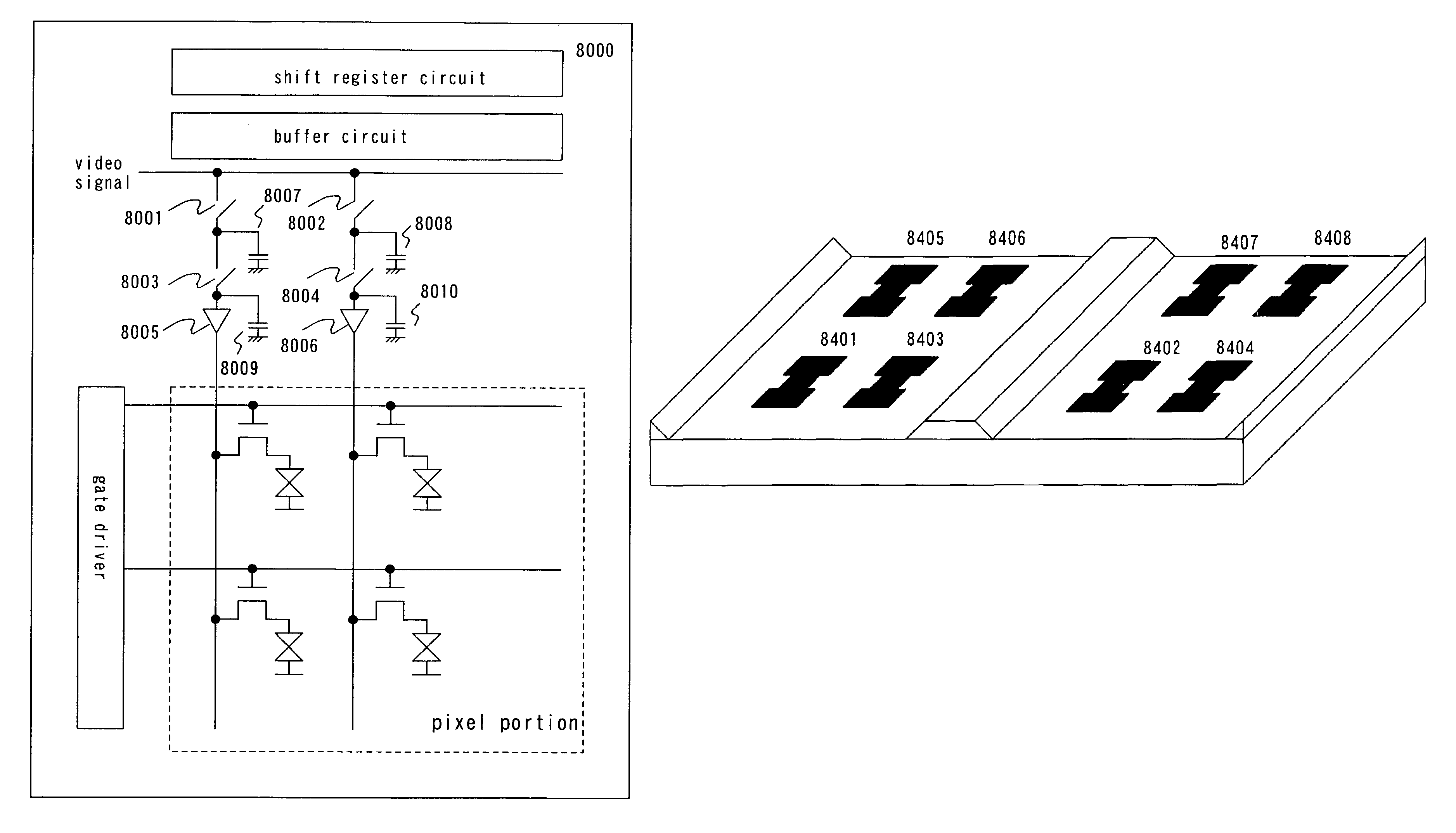
[0103]FIGS. 14A and 14b show an embodiment of a DA converting circuit in the case where a driver having the DA converting circuit is integrally formed on a substrate. FIG. 14A shows a current output type 3-bit DA converting circuit. Although in FIG. 14, the 3-bit DA converter is shown, the present invention is not limited to 3 bits. The DA converting circuit outputs a current by switching current sources composed of TFT through switches 8410, 8411, and 8412. Here, in order to keep the linearity of DA conversion, matching of TFTs 8401 to 8408 is important. Thus, an arrangement shown in FIG. 14B is used to attain such TFT matching. When necessary matching of eight TFTs is conducted, they are divided into four each. The respective four TFTs are arranged on the same projection. In FIGS. 14A and 14B, the TFTs are arranged on the projection. However, the arrangement is not limited to the projection and may be conducted on a depression. FIG. 18 shows an example in which the TFTs 8401 to 84...


PUM

PropertyMeasurementUnit
driving voltageaaaaaaaaaa
voltageaaaaaaaaaa
lengthaaaaaaaaaa

Abstract

In display devices using thin film transistors, a graphoepitaxy is used for a semiconductor layer crystallizing process. Thus, a display device in which crystallinity is improved, a variation in characteristics of thin film transistors is reduced, display nonuniformity is less, and a display quality is superior is provided. Steps are formed on a substrate in advance and an amorphous silicon film is formed thereon, and then laser crystallization is conducted in a direction perpendicular to the steps.

Description

BACKGROUND OF THE INVENTION[0001]1. Field of the Invention[0002]The present invention relates to a display device, particularly, to a display device using a thin film transistor formed on the transparent substrate such as glass or plastic. Further, it relates to an electronic apparatus using the display device.[0003]2. Description of the Related Art[0004]In recent years, a cellular phone has been becoming popular by developing communication technology. In future, electrical transmission of moving pictures and transmission of a large quantity of information will be expected. With being lightened, a mobile personal computer is into production. An information device called a personal digital assistant (PDA) developed from electrical books is produced and becoming popular. With developing a display device and the like, most of such portable information devices are equipped with flat displays.[0005]The latest technology aims at using an active matrix display device as a display device us...

Claims


Application Information

Patent Timeline
Patent Type & Authority Patents(United States)
IPC IPC(8): H01L29/00H01L29/94H01L33/00G02F1/1368G02F1/133G02F1/167G09F9/30H01L21/20H01L21/336H01L21/77H01L27/12H01L27/32H01L29/786
CPCH01L29/78696H01L29/78675H01L29/66757H01L27/1296H01L27/3244H10K59/12
Inventor KOYAMA, JUNISOBE, ATSUOSHIBATA, HIROSHIYAMAZAKI, SHUNPEI
Owner SEMICON ENERGY LAB CO LTD
Why Eureka
Try Eureka