Dynamic semiconductor storage device

a memory device and semiconductor technology, applied in static storage, digital storage, instruments, etc., can solve the problems of reducing the power dissipation of integrated circuits in battery-driven equipment, such as a cellular telephone or a personal digital assistant, a significant challenge, and a large chip size, so as to reduce the refresh current of the entire memory cell array

Inactive Publication Date: 2007-12-25
INT BUSINESS MASCH CORP
View PDF9 Cites 2 Cited by
  • Summary
  • Abstract
  • Description
  • Claims
  • Application Information

AI Technical Summary

Benefits of technology

[0011]Still another object of the present invention is to provide a dynamic semiconductor memory device that fulfills the above objects by a simple circuit configuration.
[0013]In the dynamic semiconductor memory device, the frequency of a block selection signal is divided by a preset frequency dividing ratio. If the frequency dividing ratio is 1, then the block selection signal is not divided, so that the associated block will be selected at a normal interval. If the frequency dividing ratio is 1 / 2, then the block selection signal is divided by 1 / 2, so that the associated block will be selected at an interval that is half the normal interval. Hence, the refresh cycle of this block will be half the normal interval, thus reducing the refresh current. The frequency dividing ratio is not particularly limited to 1 / 2, and an arbitrary ratio, such as 1 / 4 or 1 / 8, may be used. Moreover, the refresh current is reduced merely by adding a refresh cycle control circuit, allowing the dynamic semiconductor memory device in accordance with the present invention to be achieved by a simple circuit implementation.
[0015]In this dynamic semiconductor memory device, the memory cell array is hierarchically divided into blocks, and the refresh cycles are hierarchically set for each block. This arrangement permits detailed setting of refresh cycles, resulting in further reduced refresh current of the entire memory cell array.

Problems solved by technology

Reducing power dissipation of integrated circuits in battery-driven equipment, such as a cellular telephone or a personal digital assistant (PDA), is a significant challenge.
As such, fabricating a 32-Mbit or 64-Mbit SRAM using current wiring technology of about 0.2 μm to about 0.13 μm inevitably results in an excessively large chip.
Consequently, from the viewpoint of area efficiency, SRAMs are inferior to DRAMs, and the disadvantage of poor area efficiency ultimately inhibits continued process technology scaling.
The DRAMs, however, require stored data to be refreshed, resulting in a considerably larger standby current than for SRAM arrays.
Even this product, however, has not achieved satisfactory reduction in power consumption.
Furthermore, memory cells having such short data retention rates usually exhibit one or more defects and are replaced by redundant memory cells and not actually used.
The study of the capability distribution of data retention rates described above reveals that the majority of memory cells are refreshed more frequently than necessary, wasting a considerable amount of power.
However, setting a refresh cycle based on the capability value of each memory cell would require a circuit of an enormous scale and complexity, rendering such a solution infeasible.
In these inventions, however, the number of arrays is small, so that a satisfactory result cannot be obtained if memory cells having comparably short values of data retention rate are scattered among all arrays.

Method used


Image

  • Dynamic semiconductor storage device
  • Dynamic semiconductor storage device
  • Dynamic semiconductor storage device

Examples


first embodiment

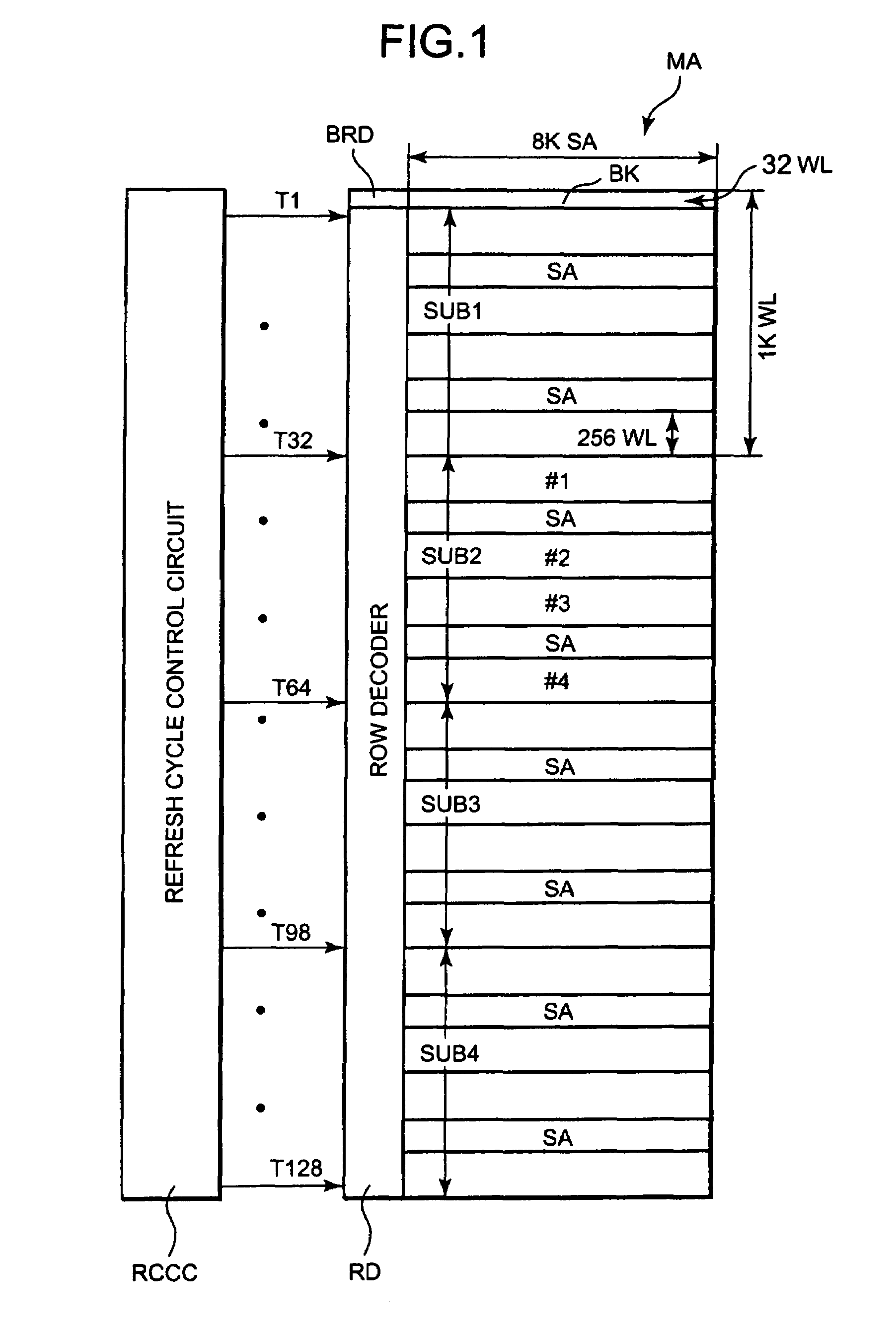
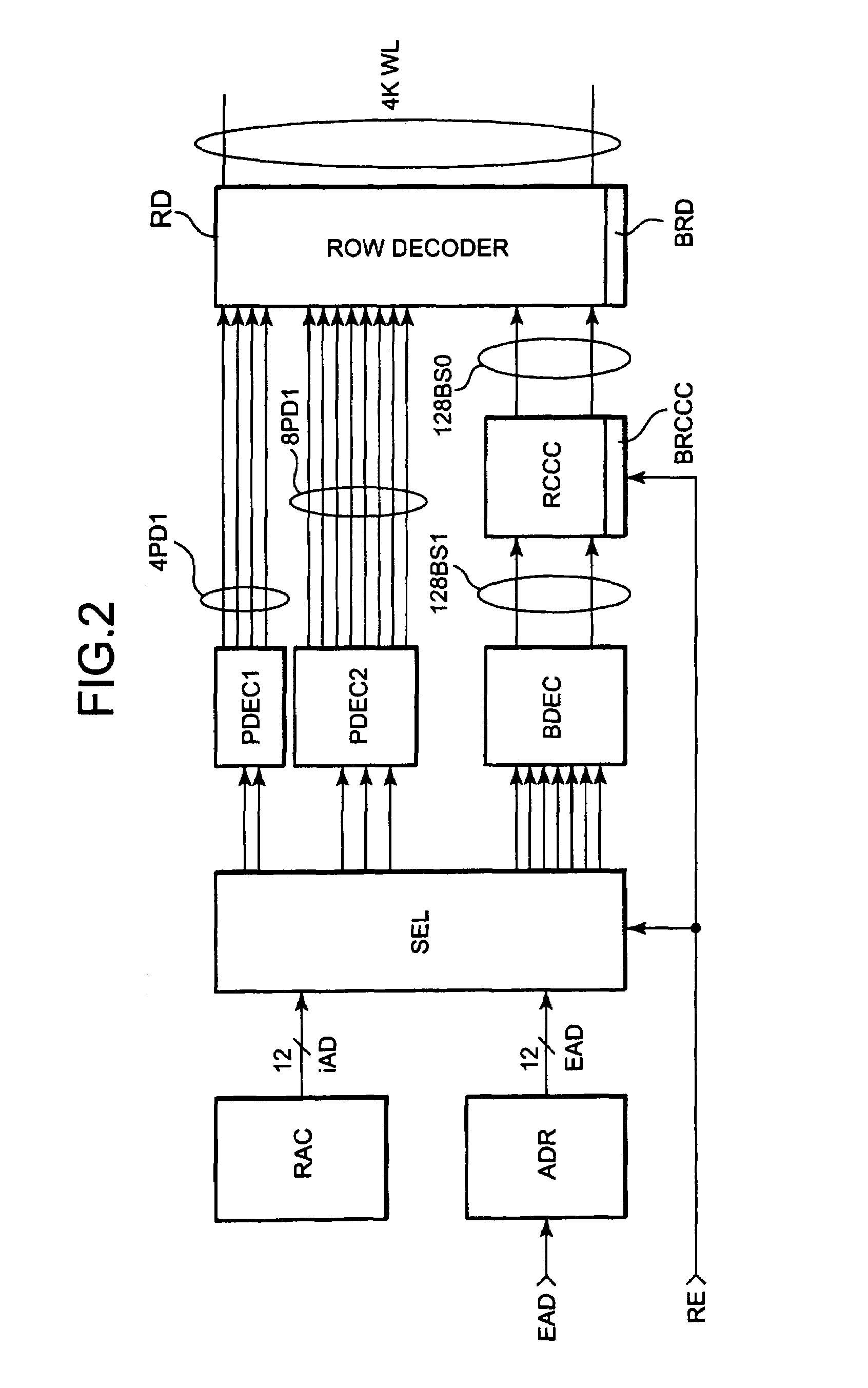
[0030]Referring to FIG. 1, a DRAM in accordance with the present invention has a 32-Mbit memory cell array MA, a row decoder RD, and a refresh cycle control circuit RCCC. The memory cell array MA is divided into four subarrays SUB 1 through SUB 4. Each of the subarrays SUB 1 through SUB 4 includes 8M (=8×220) memory cells (not shown) disposed in rows and columns, 1K (=210) word lines WL disposed in rows, 8K (=8×210) bit line pairs BL disposed in columns, and 8K sense amplifiers SA provided in association with the bit line pairs BL.

[0031]Each of the subarrays SUB 1 through SUB 4 is further divided into four regions #1 through #4, each of regions #1 through #4 including 256 word lines WL. The 4K sense amplifiers SA out of the 8K are disposed between regions #1 and #2 and another 4K sense amplifiers SA are disposed between regions #3 and #4. The entire memory cell array MA is further divided into 128 blocks BK, each block BK including 32 word lines WL.

[0032]To match the 128 blocks BK, ...

second embodiment

[0068]Referring to FIG. 6, a DRAM according to the present invention has two memory cell arrays MA. Each memory cell array MA includes 32M memory cells (not shown) arranged in rows and columns, 16K word lines WL arranged in rows, and 2K bit line pairs BL arranged in columns. Each memory cell array MA has 32-Mbit memory capacity. The entire DRAM has a 64-Mbit memory capacity. Each memory cell array MA is divided into 64 subarrays SUB, each subarray SUB having 512-Kbit memory capacity.

[0069]Referring to FIG. 7, each subarray SUB has 512K memory cells (not shown), 256 word lines WL, and 2K bit line pairs BL. 2K sense amplifiers SA are individually connected to the 2K bit line pairs BL.

[0070]As shown in FIG. 7, a row-based peripheral circuit is disposed between the two, upper and lower, memory cell arrays MA shown in FIG. 6. The row-based peripheral circuit has a refresh cycle control circuit RCCC, two row decoders RD, two virtual word line decoder and word line drivers (hereinafter ref...

third embodiment

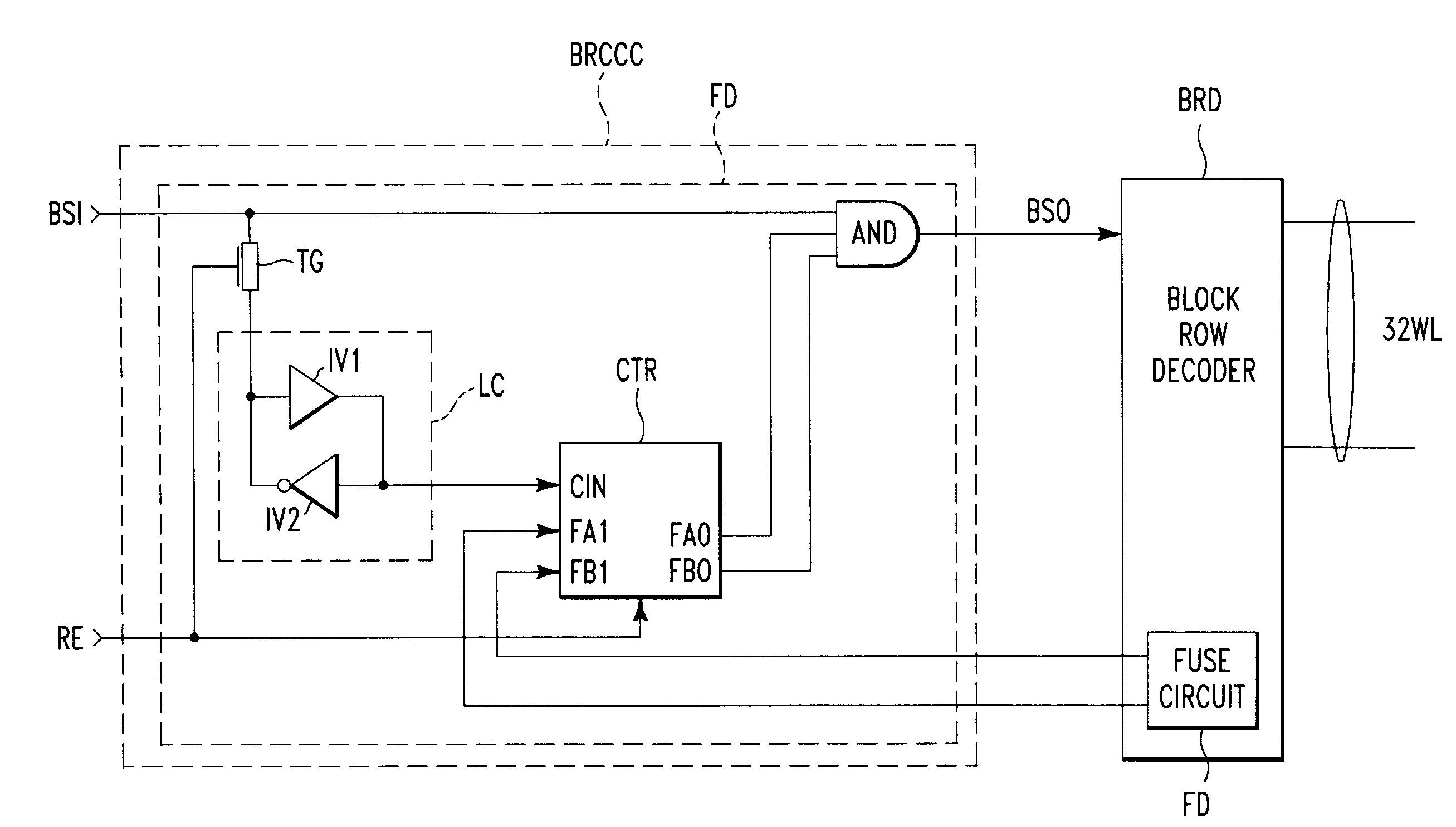
[0103]Referring to FIG. 11, the third embodiment has the fuse circuit FC0, but does not have the frequency divider FD0. Therefore, input predecode signal ZLI0 is always supplied directly to a row decoder RD as a predecode signal ZL0. A fuse signal FI0 output from a fuse circuit FC0 is supplied to all eight counters CTR1 to CTR8. When the fuse circuit FC0 is cut off and a fuse signal FI0 is switched to the H level, the counters CTR1 to CTR8 enable counter output signals Cout01 to Cout08 of LSB. When fuse circuits FC1 to FC8 are cut off and fuse signals FI1 to FI8 are switched to the H level, the counters CTR1 to CTR8 enable counter output signals Cout11 to Cout18 of MSB.

[0104]If a retention test result indicates that the shortest data retaining time of all blocks BK1 to BK8 is 128 ms or more, then the fuse circuit FC0 is cut off. If the shortest data retention time of, for example, block BK8 is 256 ms or more, then the fuse circuit FC8 is also cut off. In this case, the counter outpu...


PUM


Abstract

To achieve, by a simple circuit configuration, a DRAM that permits refresh current to be effectively reduced by selectively setting refresh cycles. A memory cell array is divided into 64 subarrays, and each subarray is further divided into 8 blocks. A refresh cycle control circuit has a fuse circuit for setting a frequency dividing ratio of 1 or 1 / 2, a frequency divider that divides the frequency of a predecode signal by the set frequency dividing ratio, fuse circuits for setting a frequency dividing ratio of 1 or 1 / 4, and frequency dividers for dividing predecode signals by the set frequency dividing ratio. The refresh cycle control circuit is capable of setting a 64-ms or 128-ms refresh cycle for the 64 subarrays and a 64-ms or 256-ms refresh cycle for 512 blocks.

Description

CROSS REFERENCE TO RELATED APPLICATIONS AND INCORPORATION BY REFERENCE[0001]This application is based upon and claims the benefit of priority of a 371 of PCT / JP04 / 05275 filed Apr. 13, 2004. This application also claims the benefit of priority from Japanese Patent Application 2003110319 filed on Apr. 15, 2003; the entire contents of which are incorporated by reference herein.FIELD OF THE INVENTION[0002]The present invention relates to a dynamic semiconductor memory device and, more particularly, to a dynamic random access memory (DRAM) in which a refresh cycle interval is selectively controlled to reduce power dissipation.BACKGROUND OF THE INVENTION[0003]Reducing power dissipation of integrated circuits in battery-driven equipment, such as a cellular telephone or a personal digital assistant (PDA), is a significant challenge. Previously, static random access memories (SRAMs) have been used extensively in semiconductor memory applications, because a SRAM memory cell typically has six ...

Claims


Application Information

Patent Timeline
Patent Type & Authority Patents(United States)
IPC IPC(8): G11C7/00G11C11/406
CPCG11C11/406G11C8/10G11C8/12G11C11/4076G11C11/4087
Inventor HOSOKAWA, KOHJIMIYATAKE, HISATADASUNAGA, TOSHIO
Owner INT BUSINESS MASCH CORP
Why Eureka
Try Eureka