Defect reduction in electrodeposited copper for semiconductor applications

a technology of electrodeposited copper and semiconductors, applied in semiconductor devices, printed circuits, printed circuit manufacturing, etc., can solve the problems of adversely affecting the conductivity of deposited copper, internal voiding and voiding, and severe penalization of the overall performance of the structure, so as to improve the macro-scale planarity of the wafer, improve the morphology of the surface, and reduce the roughness of the surface. , the effect of uneven growth

Inactive Publication Date: 2008-01-08
MACDERMID ENTHONE INC
View PDF20 Cites 27 Cited by
  • Summary
  • Abstract
  • Description
  • Claims
  • Application Information

AI Technical Summary

Benefits of technology

[0009]It is an object of the invention, therefore, to provide a method and compositions for electroplating copper to fill submicron-sized features of integrated circuit devices with fewer defects and improved surface morphology.
[0010]Briefly, therefore, the invention is direct to a method for electroplating a copper deposit onto a semiconductor integrated circuit device substrate having submicron-sized features. The method involves immersing the substrate into an electroplating bath including ionic copper and an effective amount of a defect reducing agent; and electroplating the copper deposit from the bath onto the substrate to fill the submicron-sized reliefs. The occurrence of protrusion defects from superfilling, surface roughness, and voiding due to uneven growth are reduced, and macro-scale planarity across the wafer is improved.
[0011]In another aspect, the invention is directed to a concentrate for preparation of a copper electroplating bath for electroplating a copper deposit onto a semiconductor integrated circuit device substrate having submicron-sized features. The concentrate has a defect reducing agent which reduces the occurrence of protrusion defects from superfilling, surface roughness, and voiding due to uneven growth, and improves macro-scale planarity across the wafer.

Problems solved by technology

The trend to smaller chip sizes and increased circuit density requires the miniaturization of interconnect features which severely penalizes the overall performance of the structure because of increasing interconnect resistance and reliability concerns such as electromigration.
Other micro-defects which adversely affect conductivity in deposited copper result from internal voiding and voiding attributable to detachment of the deposited copper from the walls of features including vias and trenches.

Method used


Image

  • Defect reduction in electrodeposited copper for semiconductor applications
  • Defect reduction in electrodeposited copper for semiconductor applications
  • Defect reduction in electrodeposited copper for semiconductor applications

Examples


Embodiment Construction

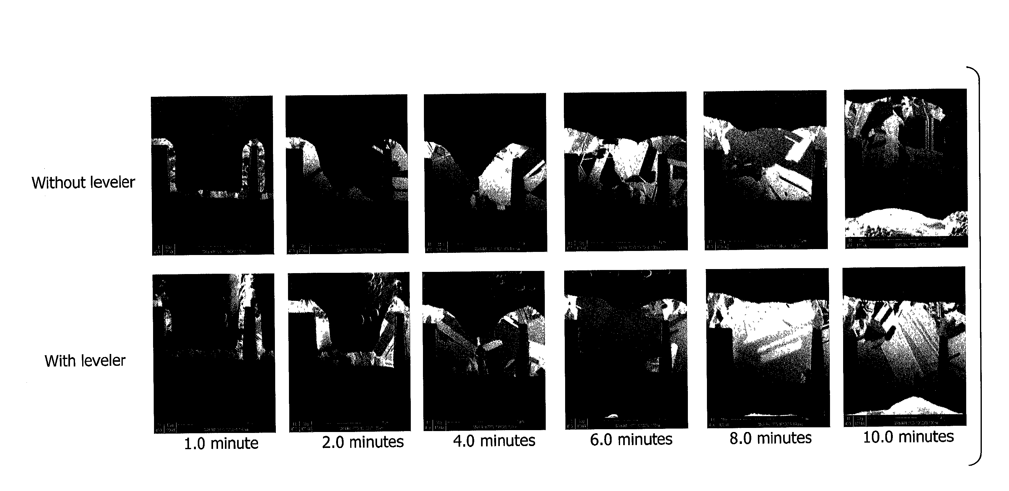
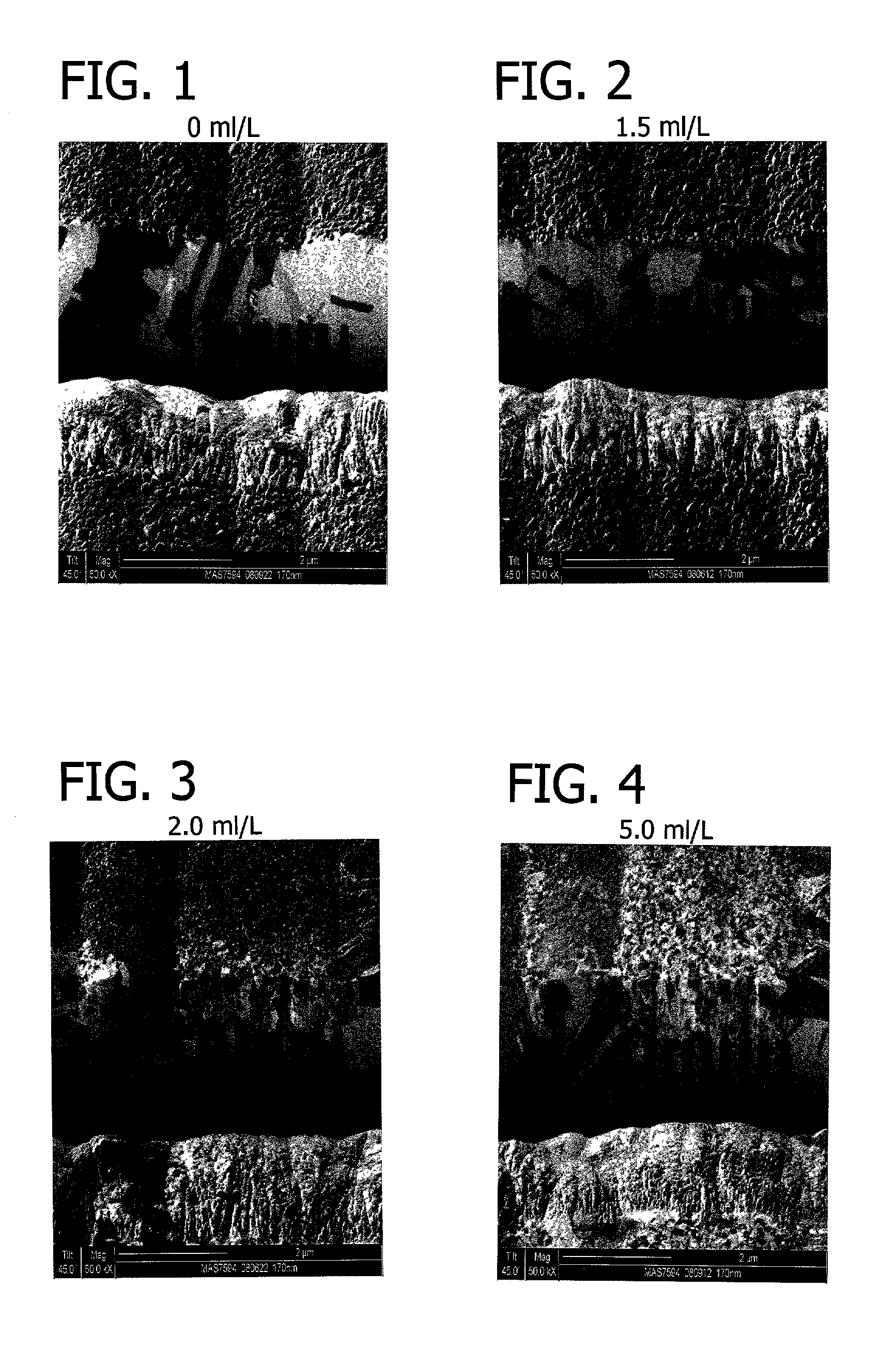
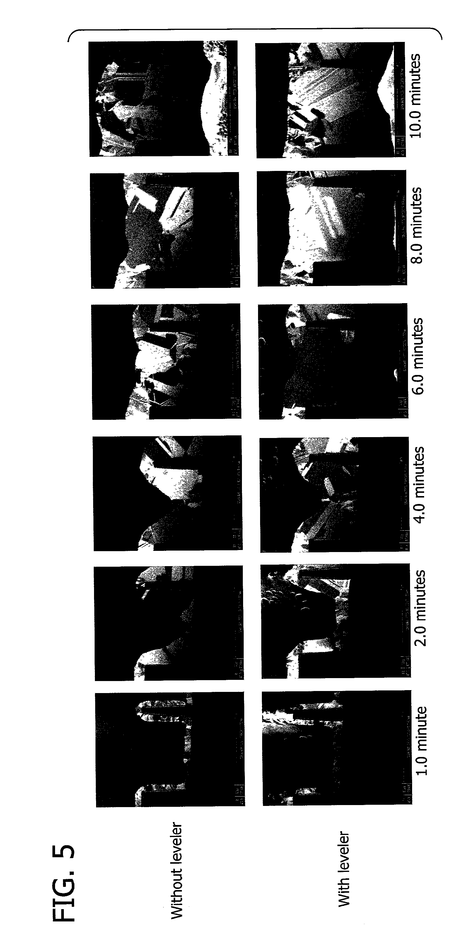
[0016]In accordance with this invention, a compound is incorporated into the plating bath which has the effect of reducing formation of micro-defects. Certain defects in deposited copper can occur due to locally uneven growth of copper crystals. Other defects formed after deposition, applicants believe, can be attributed to recrystallization and grain growth in the deposit. In particular, there are changes in volume resulting from grain growth, which changes in volume produce stress-induced defects. These volume changes also cause a degree of detachment of the deposit from the via and trench walls, which constitute defects. And recrystallization causes spontaneous internal voids as grain boundaries are eliminated.

[0017]Superfilling is rapid bottom up deposition within the features which is created by a two additive system consisting of a suppressor and accelerator. Generally the bottom-up filling created by a two-part system tends to form a bump or protruding surface defect over the...


PUM

PropertyMeasurementUnit
thicknessaaaaaaaaaa
thicknessaaaaaaaaaa
concentrationaaaaaaaaaa

Abstract

A method for electroplating a copper deposit onto a semiconductor integrated circuit device substrate having submicron-sized features, and a concentrate for forming a corresponding electroplating bath. A substrate is immersed into an electroplating bath formed from the concentrate including ionic copper and an effective amount of a defect reducing agent, and electroplating the copper deposit from the bath onto the substrate to fill the submicron-sized reliefs. The occurrence of protrusion defects from superfilling, surface roughness, and voiding due to uneven growth are reduced, and macro-scale planarity across the wafer is improved.

Description

BACKGROUND OF THE INVENTION[0001]This invention relates to a method, compositions, and additives for electrolytic copper metallization of silicon wafers in the manufacture of semiconductor integrated circuit (IC) devices.[0002]The demand for manufacturing semiconductor IC devices such as computer chips with high circuit speed, high packing density and low power dissipation requires the downward scaling of feature sizes in ultra-large-scale integration (ULSI) and very-large-scale integration (VLSI) structures. The trend to smaller chip sizes and increased circuit density requires the miniaturization of interconnect features which severely penalizes the overall performance of the structure because of increasing interconnect resistance and reliability concerns such as electromigration.[0003]Traditionally, such structures had used aluminum and aluminum alloys as the metallization on silicon wafers with silicon dioxide being the dielectric material. In general, openings are formed in the...

Claims


Application Information

Patent Timeline
Patent Type & Authority Patents(United States)
IPC IPC(8): C25D5/02C25D3/38C25D7/12H01L21/288
CPCC25D3/38C25D7/12H01L21/2885H01L21/76877H05K3/423C25D7/123
Inventor COMMANDER, JOHNHURTUBISE, RICHARDPANECCASIO, VINCENTLIN, XUANJIRAGE, KSHAMA
Owner MACDERMID ENTHONE INC
Why Eureka
Try Eureka