Active organic electroluminescence panel display with blank layer covering contact opening

a technology of active organic and electroluminescence panel, applied in the field of display, can solve the problems that the crt still has some issues that need to be resolved, affecting the performance of the device, etc., and achieve the effect of avoiding the shorting of the anode and cathode layers

Active Publication Date: 2008-01-08
AU OPTRONICS CORP
View PDF10 Cites 18 Cited by
  • Summary
  • Abstract
  • Description
  • Claims
  • Application Information

AI Technical Summary

Benefits of technology

[0010]Therefore, an object of the present invention is to provide an active organic electroluminescence panel display and a fabricating method thereof for avoiding the shorting of the anode and cathode layers at the place corresponding to the contact opening and the edge of the source / drain terminals.
[0011]The other object of the present invention is to provide an active organic electroluminescence panel display and a fabricating method thereof for avoiding the damage resulting from the use of a shadow mask directly contacting the substrate for forming the organic luminescent layer.
[0016]Accordingly, the present invention forms the blank layer at the place corresponding to the contact openings and the edge of the source / drain terminals for planarizing the structure of the panel. The step height of the structure can be reduced and the shorting of the anode and cathode layers resulting from the over-thick organic luminescent layer thereat can be avoided. Additionally, the present invention uses the blank layer for supporting the shadow mask during the deposition the organic luminescent layer. Therefore, the damage resulting from the contact between the shadow mask and the organic luminescent layer during the deposition process thereof can be evaded.

Problems solved by technology

However, because of space restriction, power consumption and environmental concern, CRT still has some issues that need to be resolved.
During the sputtering processes, because the shadow mask is repeatedly made to come in contact to and then separated from the TFT substrate, damage will result therefrom adversely affecting the performance of the device.

Method used


Image

  • Active organic electroluminescence panel display with blank layer covering contact opening
  • Active organic electroluminescence panel display with blank layer covering contact opening
  • Active organic electroluminescence panel display with blank layer covering contact opening

Examples


Embodiment Construction

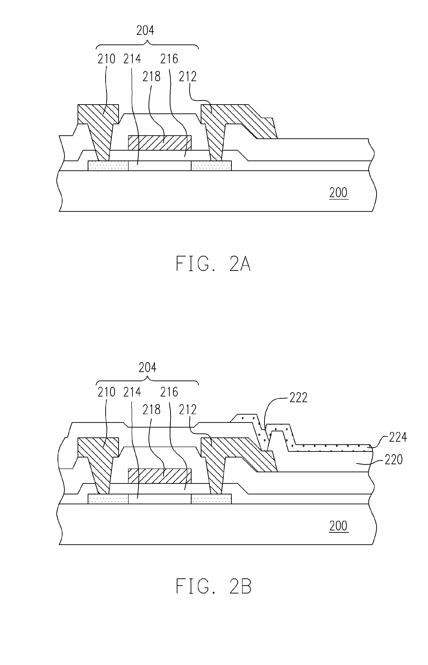
[0026]FIGS. 2A-2F is a schematic process flowchart illustrating a process of fabricating an active organic electroluminescence panel display according to a preferred embodiment of the present invention. FIG. 4A is a top view of FIG. 2A. FIGS. 2A and 2B are the cross-sectional views taken along I-I″ in FIG. 4A.

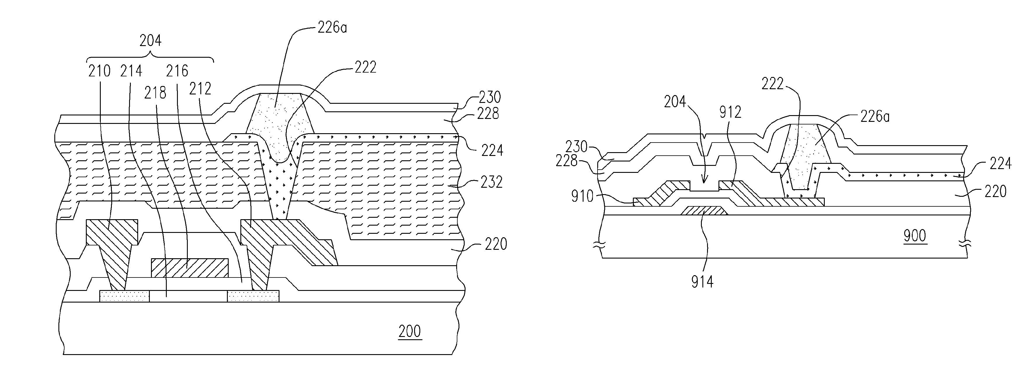
[0027]Referring to FIGS. 2A and 4A, a thin film transistor array 202 is formed on a substrate 200, wherein the thin film transistor array 202 comprises a plurality of thin film transistors 204, a plurality of scan lines 206 and a plurality of data lines 208. The thin film transistor 204 can be, for example, a polysilicon thin film transistor, which comprises a source terminal 210, a drain terminal 212, a channel 214, a gate dielectric layer 216 and a gate terminal 218. The scan lines 206 of the thin film transistor array 202 electrically connect with the gate terminal 218 and the data lines 208 electrically connect with the source 210.

[0028]Moreover, in addition to being formed...


PUM


Abstract

An active organic electroluminescence panel display and a fabricating method thereof are disclosed. A thin film transistor array comprising a plurality of thin film transistors, a plurality of datalines and a plurality of scanlines are formed on a substrate. A passivation layer is formed on the substrate, covering the thin film transistor array. A contact opening is formed in the passivation layer for exposing a prescribed area of the array. An anode layer is formed on the passivation layer and fills into the contact opening. A blank layer is formed on the anode, covering the contact opening. A shadow mask is disposed on the blank layer. Then, a sputtering process is performed to form an organic luminescent layer. The shadow mask is then removed, and a cathode layer is formed on the organic luminescent layer for forming an active organic electroluminescence panel display.

Description

CROSS REFERENCE TO RELATED APPLICATIONS[0001]This application claims the priority benefit of Taiwan application serial no. 92130175, filed on Oct. 30, 2003.BACKGROUND OF INVENTION[0002]1. Field of the Invention[0003]The present invention relates to a display and a fabricating method thereof, and more particularly to an active organic electroluminescence panel display and a fabricating method thereof.[0004]2. Description of the Related Art[0005]Because of the shrinkage of semiconductor device and displays, portable devices are now available to consumers. As to displays, cathode ray tubes (CRT) dominate the market because of its high image quality and low cost. However, because of space restriction, power consumption and environmental concern, CRT still has some issues that need to be resolved. Therefore, thin film transistor liquid crystal display, which offers high image quality, small space occupation, low power consumption and radiation free, has gradually replaced CRT.[0006]Flat ...

Claims


Application Information

Patent Timeline
Patent Type & Authority Patents(United States)
IPC IPC(8): H01J1/62H01J63/04H01L27/32H01L51/52H05B33/00H05B33/10
CPCH01L27/3248H01L27/3246H01L51/5203H10K59/122H10K59/123H10K59/805H10K50/805
Inventor CHEN, YUN-SHENG
Owner AU OPTRONICS CORP
Why Eureka
Try Eureka