
Memory device using nanotube cells

a memory device and nanotube technology, applied in nanoinformatics, instruments, animal intestines working up, etc., can solve the problems of junction leakage current generation and difficulty in satisfying the refresh characteristic of dram cells, and achieve the effect of reducing the capacitance of each cell and reducing the size of a capacitor

Inactive Publication Date: 2008-02-26
SK HYNIX INC
View PDF13 Cites 19 Cited by
  • Summary
  • Abstract
  • Description
  • Claims
  • Application Information

AI Technical Summary

Benefits of technology

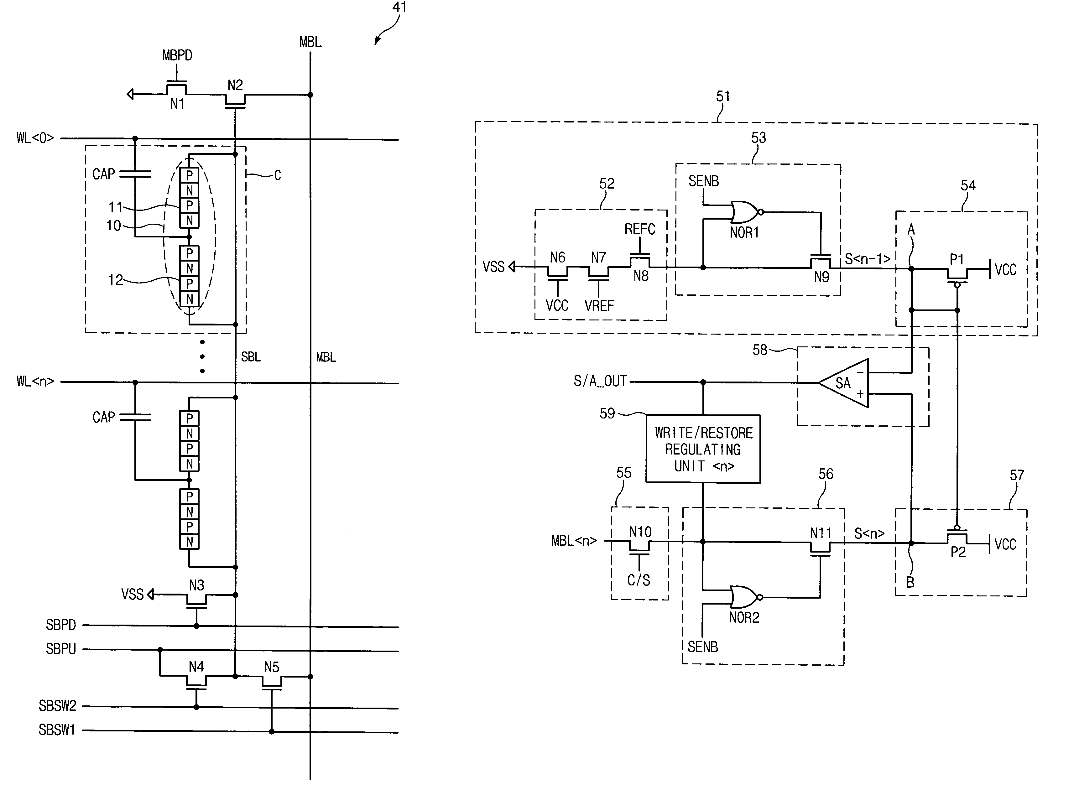
The present invention provides a DRAM with a hierarchical bit line structure that reduces capacitance per cell, making it smaller. It also uses a nano tube sub cell array that does not require an additional gate control signal, reducing the size of the memory. The nano tube sub cell array includes a capacitor and a PNPN nano tube switch, which improves operation characteristics of memory cells. The memory device using a nano tube cell has a hierarchical bit line structure and includes a cell array block and a sense amplifier array. The plurality of unit nano tube cells each comprises a capacitor and a PNPN nano tube switch. The PNPN nano tube switch selectively switches based on voltage applied to the word line and the sub bit line.

Problems solved by technology

As a result, it is difficult to satisfy the refresh characteristic of the DRAM cell.
Also, junction leakage current is generated in a storage node terminal which occupies a relatively large area in the DRAM cell.

Method used


Image

  • Memory device using nanotube cells
  • Memory device using nanotube cells
  • Memory device using nanotube cells

Examples


Embodiment Construction

[0024]The present invention will be described in detail with reference to the accompanying drawings.

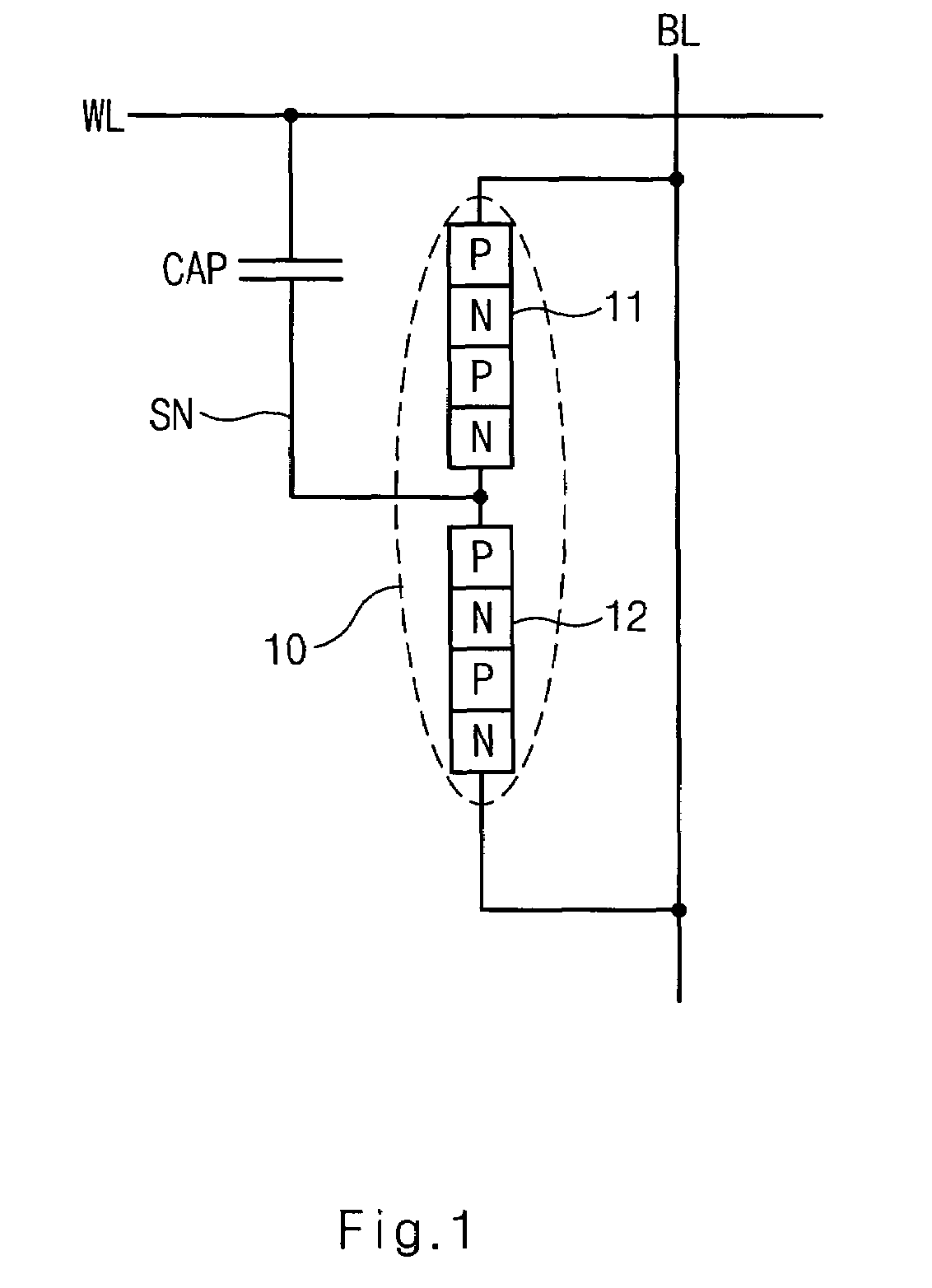
[0025]FIG. 1 is a diagram illustrating a unit nano tube cell according to an embodiment of the present invention.

[0026]In an embodiment, the unit nano tube cell comprises a capacitor CAP and a PNPN nano tube switch 10. Here, the PNPN nano tube switch 10 comprises PNPN diode switches 11 and 12. The PNPN diode switches 11 and 12 are connected in parallel between a bit line BL and a bottom electrode of the capacitor CAP.

[0027]The PNPN diode switch 11 is connected backward between the bit line BL and one electrode of the capacitor CAP, and the PNPN diode switch 12 is connected forward between the bit line BL and one electrode of the capacitor CAP. The other electrode of the capacitor CAP is connected to a word line WL.

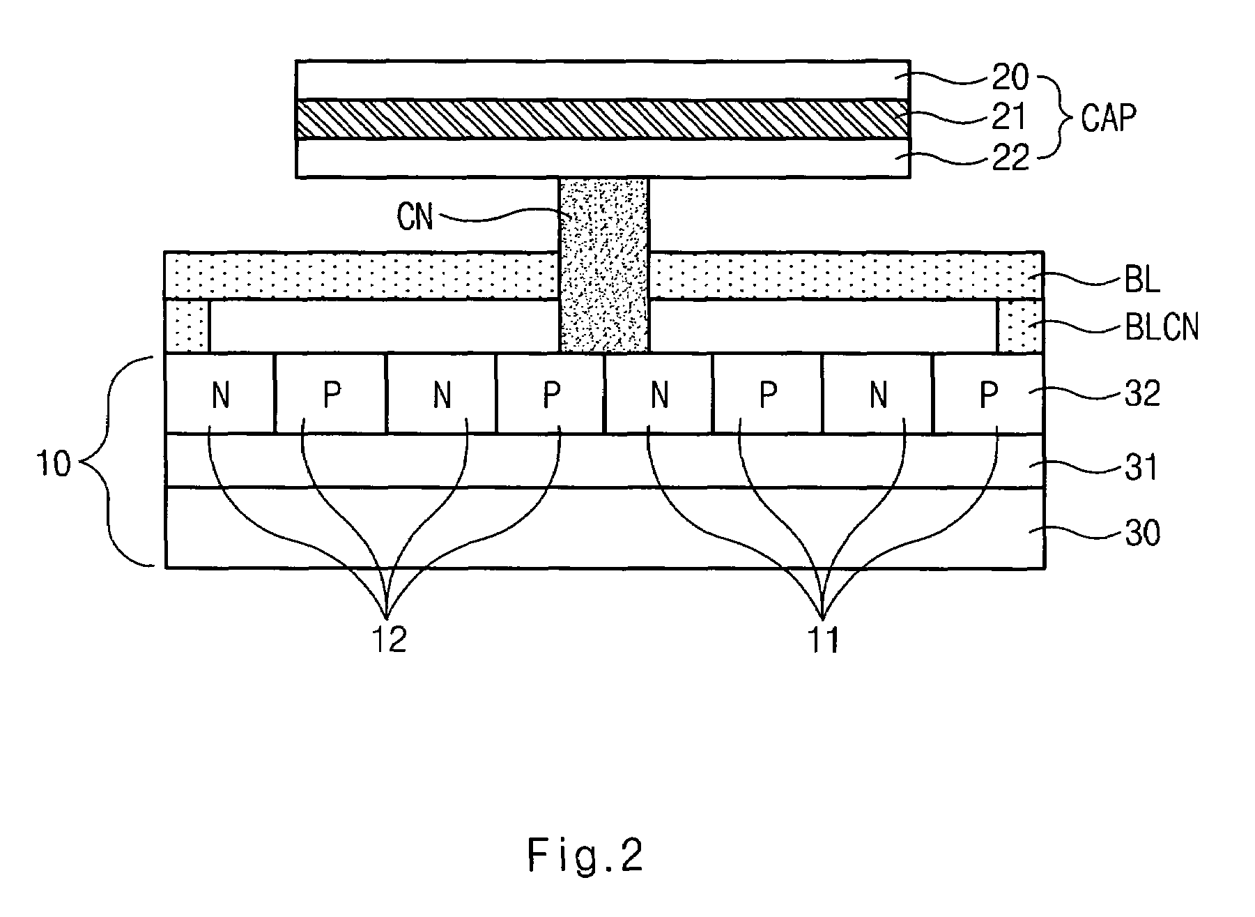
[0028]FIG. 2 is a cross-sectional diagram illustrating the nano tube cell of FIG. 1.

[0029]The PNPN nano tube switch 10 comprises an insulating layer 31 formed on a silicon s...


PUM


Abstract

A memory device using a nanotube cell comprises a plurality of nanotube sub-cell arrays each having a hierarchical bit line structure including a main bit line and a sub-bit line. In the memory device, a nanotube cell array comprising a capacitor and a PNPN nanotube switch which does not require an additional gate control signal is located between a word line and the sub-bit line, so that a cross point cell array is embodied to reduce the whole chip size.

Description

BACKGROUND OF THE INVENTION[0001]1. Field of the Invention[0002]The present invention generally relates to a memory device using a nano tube cell, and more specifically, to a technology of reducing the whole memory size by providing a plurality of nano tube sub cell arrays as a cross point cell in a hierarchical bit line structure including a main bit line and a sub bit line.[0003]2. Description of the Prior Art[0004]Generally, a Dynamic Random Access Memory (hereinafter, referred to as ‘DRAM’) comprises a transistor for performing a switching operation depending on a state of a word line to connect a capacitor to a bit line, and the capacitor connected between a plate line and one terminal of the transistor.[0005]Here, a switching device of a conventional DRAM cell is a NMOS transistor whose switching operation is controlled by a gate control signal. However, when a cell array is embodied by using the NMOS transistor as a switching device, the whole chip size is increased.[0006]Mea...

Claims


Application Information

Patent Timeline
Patent Type & Authority Patents(United States)
IPC IPC(8): G11C11/39B82B1/00G11C11/4197G11C8/12G11C7/18G11C11/00G11C11/401G11C11/54G11C13/02H10B12/00
CPCB82Y10/00G11C7/18G11C11/54G11C13/003G11C13/0033G11C13/025G11C2213/74G11C2213/76Y10S977/936Y10S977/943A22C17/16A22C17/14A22B5/18
Inventor KANG, HEE BOK
Owner SK HYNIX INC
Learn More