Variable demultiplexer

a multi-layer, variable technology, applied in the direction of instruments, optical waveguide light guides, optical elements, etc., can solve the problems of low yield, prone to bad productivity, and the prior art already described suffer from the following problems, so as to improve yield and stable characteristics, reduce the size of an element, and improve the effect of yield

Inactive Publication Date: 2008-04-08
SHARP KK
View PDF9 Cites 20 Cited by
  • Summary
  • Abstract
  • Description
  • Claims
  • Application Information

AI Technical Summary

Benefits of technology

[0018]An object of the invention is to provide a small variable demultiplexer which includes a variable mechanism, and can reduce sizes of an element so that improved yield and stable characteristics can be achieved.
[0020]As described above, the invention lowers a group velocity in a traveling direction of light caused by the one-dimensional photonic crystal structure formed in the waveguide array so that elements of small sizes can be produced. Consequently, each chip can be produced by EB exposure within one field so that the characteristics are stable, and the yield is improved.

Problems solved by technology

However, the prior arts already described suffer from the following problems.
Therefore, when producing the variable demultiplexers, problems of low yield and bad productivity are liable to occur.
In particular, when producing the variable demultiplexers by Electron Beam (EB) exposure, it is impossible to produce each of chips in one field of the EB exposure step, and a field boundary is formed inside a structure of the variable demultiplexer.
This may cause unstable features in the variable demultiplexer.
In connection with the technique disclosed in Japanese Patent Laying-Open No. 2003-255160, when an AWG is once formed on a substrate, it is no longer possible to change the form of the slab waveguide on the output side and the structure of the array waveguides.
Likewise, according to the technique disclosed in Japanese Patent Laying-Open No. 2003-43277, when the photonic crystal is once produced, it is no longer possible to change the structure such as a form and a size of a hole and a grating constant of the photonic crystal.
Thus, each wavelength is output at a fixed position, and flexible switching is impossible.

Method used


Image

  • Variable demultiplexer
  • Variable demultiplexer
  • Variable demultiplexer

Examples


first embodiment

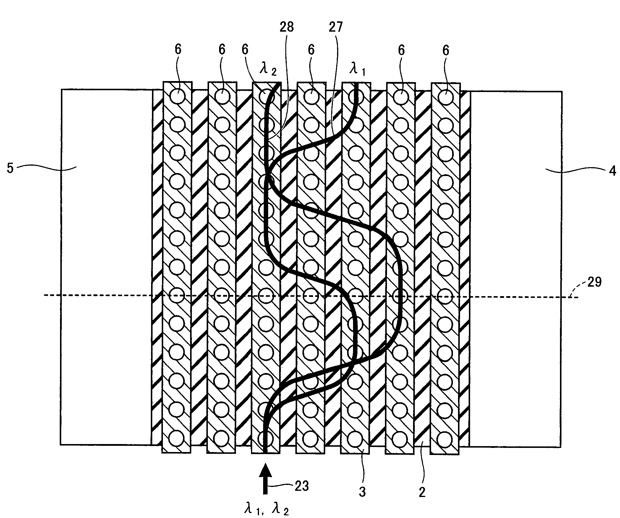
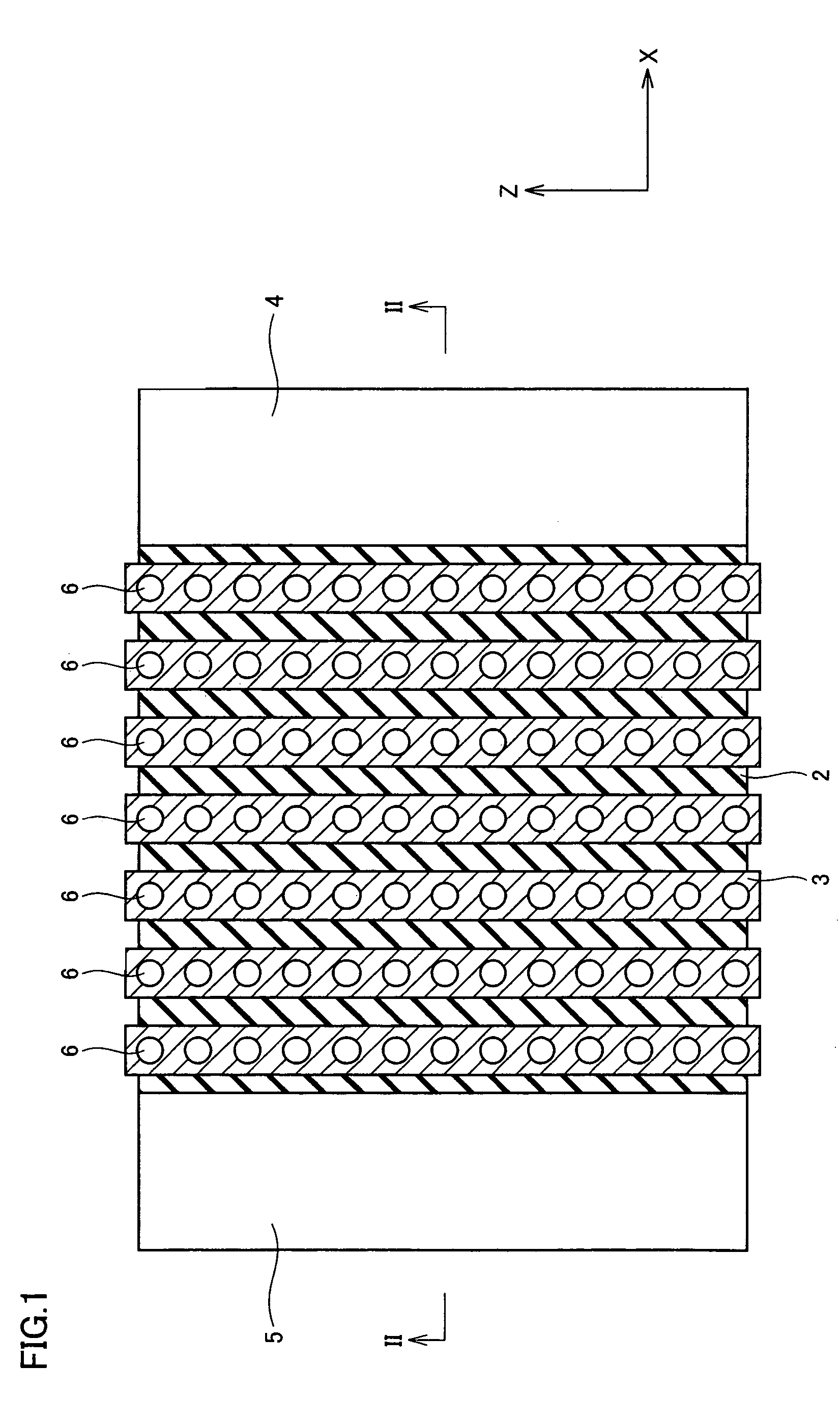
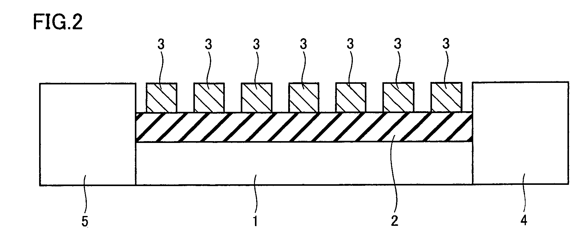
[0046]Referring to FIGS. 1 and 2, a first embodiment of a small variable demultiplexer according to the invention will now be described.

[0047]A small variable demultiplexer shown in FIGS. 1 and 2 is formed of a Si photonic wire waveguide array using an SOI (Silicon On Insulator). As shown in FIG. 2, an SiO2 layer 2 is arranged over a silicon substrate 1. A plurality of Si photonic wire waveguides 3 formed of an upper silicon layer 13 (see FIG. 3) are formed on SiO2 layer 2. The plurality of Si photonic wire waveguides 3 are parallel to each other, and extend in a Z-axis direction as can be seen from FIG. 1. The plurality of Si photonic wire waveguides 3 are spaced by a predetermined distance in an X-axis direction from each other, and are arranged in a discrete (cyclic) fashion. Thus, the plurality of Si photonic wire waveguides 3 are formed parallel to each other with substantially uniform spaces therebetween. A heater 4 and a heat sink 5 are connected to end surfaces, which are lo...

second embodiment

[0077]Referring to FIGS. 16 and 17, description will now be given on a second embodiment of the small variable demultiplexer according to the invention.

[0078]A small variable demultiplexer shown in FIG. 16 includes silicon substrate 1, SiO2 layer 2 formed on silicon substrate 1, the plurality of Si photonic wire waveguides 3 formed on SiO2 layer 2 and forming the waveguide array, and electrodes 74 formed on Si photonic wire waveguides 3. Si photonic wire waveguide 3 has substantially the same structure as Si photonic wire waveguide 3 in the small variable demultiplexer shown in FIG. 1. Each electrode 74 is provided with empty holes 6 reaching the lower surface of Si photonic wire waveguide 3. In FIG. 16, the traveling direction of the light is the Z-axis direction, a direction perpendicular to the extension direction of Si photonic wire waveguide 3 is the X-axis direction, and a direction of thickness of Si photonic wire waveguide 3 (i.e., direction perpendicular to the main surface...

third embodiment

[0082]Referring to FIGS. 18 and 19, description will now be given on a third embodiment of the small variable demultiplexer according to the invention.

[0083]A small variable demultiplexer shown in FIGS. 18 and 19 has substantially the same structure as the small variable demultiplexer shown in FIGS. 1 and 2 except for that widths W1-W7 of Si photonic wire waveguides 83, diameters of empty holes 6a-6g and spaces L1-L6 between neighboring Si photonic wire waveguides 83 are not uniform. Referring to FIG. 18, as the position moves in the X-axis direction from one end of the waveguide array on the left side in FIG. 18 toward the other end, the width (W1-W7) of Si photonic wire waveguide 83 and the diameter of empty hole (6a-6g) gradually increase. Also, the foregoing space (L1-L6) gradually decreases as the position moves in the X-axis direction from the left end toward the right end in FIG. 18. This structure of the waveguide array formed of Si photonic wire waveguides 83 is referred to...


PUM


Abstract

A small variable demultiplexer capable of improving yield and stabilizing characteristics can be obtained. The small variable demultiplexer includes an SiO2 layer serving as a base medium, a waveguide array, a heater serving as an external refractive index modulating unit and a heat sink serving as the external refractive index modulating unit. The waveguide array is arranged on the SiO2 layer. The waveguide array is formed of the plurality of Si photonic wire waveguides serving as waveguides. The heater and the heat sink provide a refractive index gradient which is formed in the direction perpendicular to the extension direction of the Si photonic wire waveguide, and is variable depending on the plurality of Si photonic wire waveguides. The Si photonic wire waveguide has a one-dimensional photonic crystal structure in the extension direction of the Si photonic wire waveguide.

Description

[0001]This nonprovisional application is based on Japanese Patent Application No. 2004-350088 filed with the Japan Patent Office on Dec. 2, 2004, the entire contents of which are hereby incorporated by reference.BACKGROUND OF THE INVENTION[0002]1. Field of the Invention[0003]The present invention relates to a variable demultiplexer, and particularly to a variable demultiplexer using optical Bloch oscillations.[0004]2. Description of the Background Art[0005]In recent years, demands for large-capacity optical communication networks have been remarkably increasing. As one of techniques for meeting such demands, there has been wavelength division multiplex transmission. For using this technique, changes have occurred in main devices, and it is now required to use optical control devices such as a variable demultiplexer. Variable demultiplexers using optical Bloch oscillations or photonic crystals have been known as the above kind of variable demultiplexers.[0006]The variable demultiplex...

Claims


Application Information

Patent Timeline
Patent Type & Authority Patents(United States)
IPC IPC(8): G02B6/28
CPCB82Y20/00G02B6/12007G02B6/1225G02F1/313G02F1/0147G02F2202/32G02F2203/585
Inventor KATO, YOSHIMICHIOKUMURA, TOSHIYUKI
Owner SHARP KK
Why Eureka
Try Eureka