GaN single crystal substrate and method of making the same

a single crystal substrate and substrate technology, applied in the direction of crystal growth process, semiconductor laser, gel state, etc., to achieve the effect of improving the characteristics of semiconductor devices, and reducing the cost of production

Inactive Publication Date: 2008-04-15
SUMITOMO ELECTRIC IND LTD
View PDF31 Cites 9 Cited by
  • Summary
  • Abstract
  • Description
  • Claims
  • Application Information

AI Technical Summary

Benefits of technology

[0010]However, the GaN substrate manufactured by the method disclosed in the above-mentioned Japanese Patent Application Laid-Open No. HEI 8-116090 has a very low crystal quality due to lattice mismatches and the like, so that large warpage occurs due to internal stress caused by crystal defects, whereby it has not been in practical use yet. Along with advances in technology, it has been required to further improve characteristics of semiconductor devices using gallium nitride type compound semiconductors, whereby it has become necessary for the inventors to produce a GaN single crystal substrate having a higher quality. To this aim, it is necessary to further reduce crystal defects such as dislocation occurring in the epitaxial layer of the GaN single crystal substrate. If crystal defects are reduced, then a GaN single crystal substrate having a high crystal quality, low internal stress, and substantially no warpage can be obtained.

Problems solved by technology

HEI 8-116090 has a very low crystal quality due to lattice mismatches and the like, so that large warpage occurs due to internal stress caused by crystal defects, whereby it has not been in practical use yet.

Method used


Image

  • GaN single crystal substrate and method of making the same
  • GaN single crystal substrate and method of making the same
  • GaN single crystal substrate and method of making the same

Examples


first embodiment

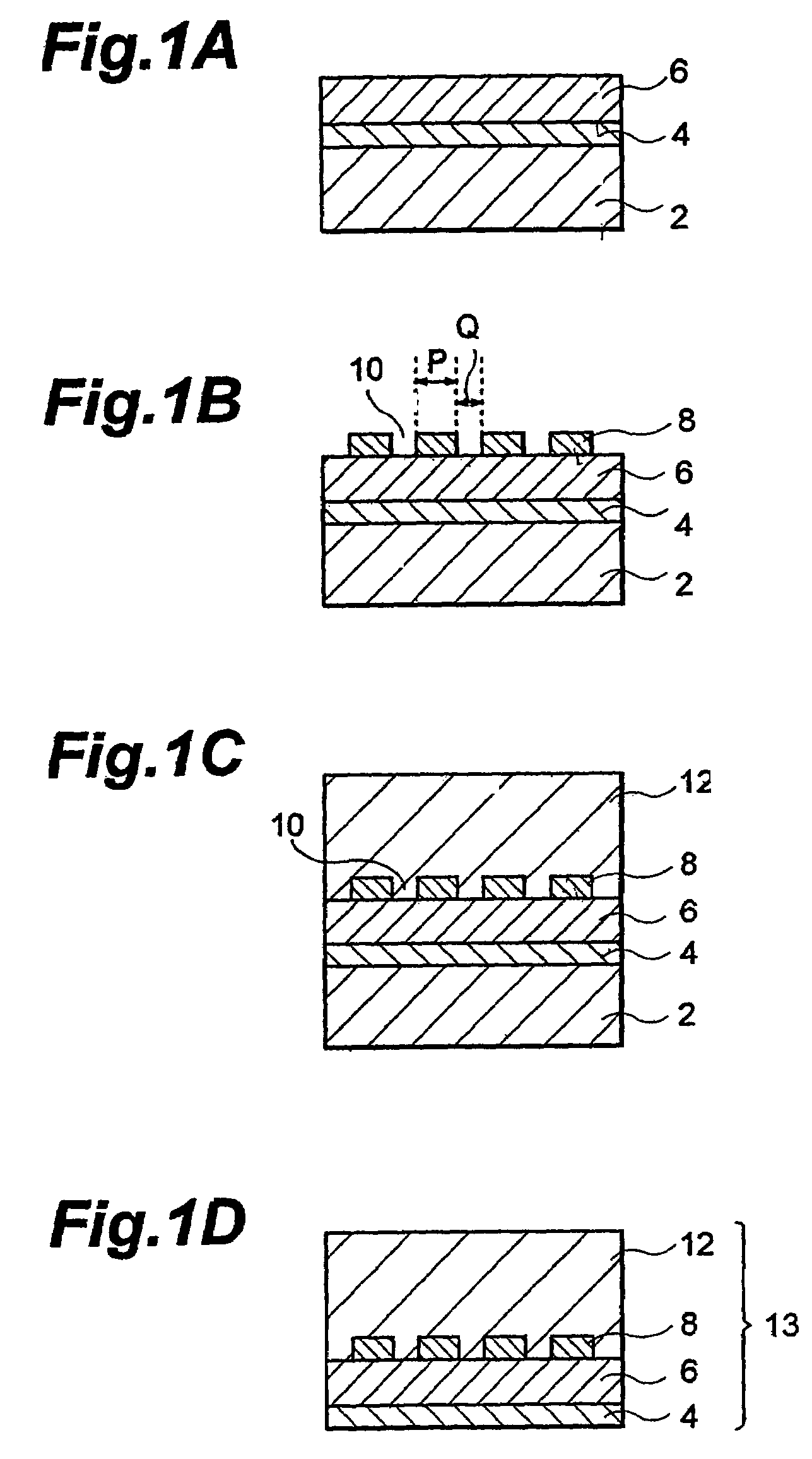
[0055]The GaN single crystal substrate in accordance with a first embodiment and a method of making the same will be explained with reference to the manufacturing step charts of FIGS. 1A to 1D.

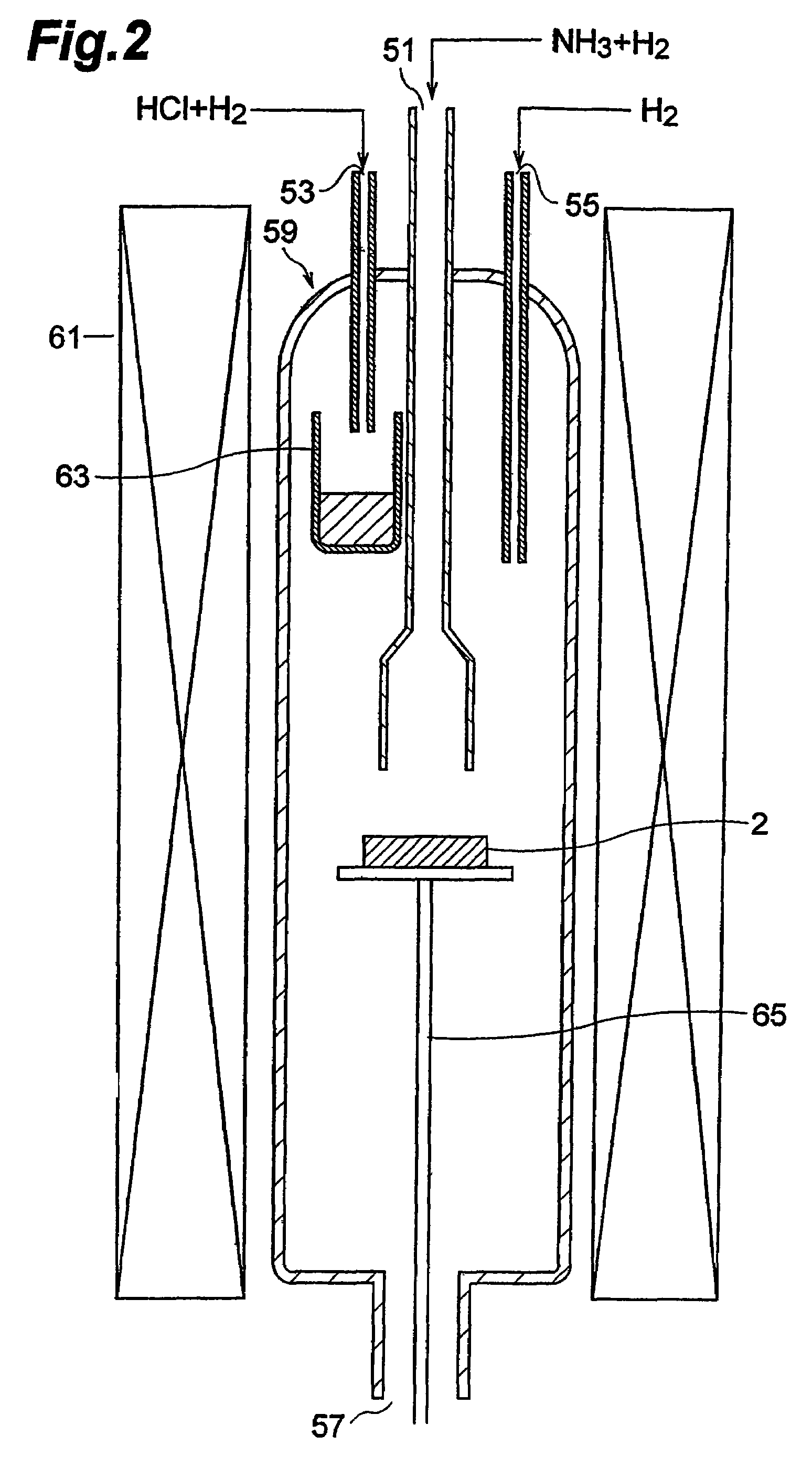
[0056]Initially, in the first step shown in FIG. 1A, a GaAs substrate 2 is installed within a reaction vessel of a vapor phase growth apparatus. Here, as the GaAs substrate 2, a GaAs(111)A substrate in which GaAs(111) plane is a Ga surface or a GaAs(111)B substrate in which GaAs(111) plane is an As surface can be employed.

[0057]After the GaAs substrate 2 is installed in the reaction vessel of the vapor phase growth apparatus, a buffer layer 4 made of GaN is formed on the GaAs substrate 2. The method of forming the buffer layer 4, includes vapor phase growth methods such as HVPE (Hydride Vapor Phase Epitaxy) method, organic metal chloride vapor phase growth method, and MOCVD method. Each of these vapor phase growth methods will now be explained in detail.

[0058]First, the HVPE method will be exp...

second embodiment

[0081]The GaN single crystal substrate in accordance with a second embodiment and a method of making the same will be explained with reference to the manufacturing step charts of FIGS. 6A to 6D.

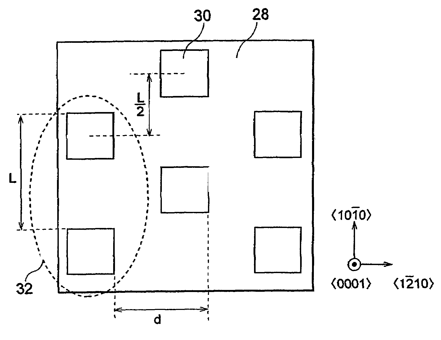
[0082]Initially, in the first step shown in FIG. 6A, a mask layer 8 made of SiN or SiO2 is directly formed on a GaAs substrate 2. For forming the mask layer 8, an SiN film or SiO2 film having a thickness of about 100 nm to about 500 nm is formed by plasma CVD or the like, and this SiN film or SiO2 film is patterned by photolithography technique.

[0083]FIG. 7 is a plan view of the wafer in the first step shown in FIG. 6A. As shown in FIGS. 6A and 7, the mask layer 8 of this embodiment is also formed with a plurality of stripe windows 10 shaped like stripes as in the first embodiment. The stripe windows 10 are formed so as to extend in the direction of the GaAs substrate 2. The arrows in FIG. 7 indicate the crystal orientations of the GaAs substrate 2.

[0084]After the mask layer 8 is formed, the...

third embodiment

[0090]Before explaining a third embodiment, how the GaN single crystal substrate and method of making the same in accordance with this embodiment have been accomplished will be explained.

[0091]For satisfying the demand for improving characteristics of optical semiconductor devices, the inventors have repeated trial and error in order to manufacture a GaN substrate having a higher quality. As a result, the inventors have found it important to reduce the internal stress of the grown GaN epitaxial layer for making a high-quality GaN substrate.

[0092]In general, the internal stress of the GaN epitaxial layer can be studied as being divided into thermal stress and true internal stress. This thermal stress occurs due to the difference in coefficient of thermal stress between the GaAs substrate and the epitaxial layer. Though the warping direction of the GaN substrate can be expected from the thermal stress, it has become clear that the true internal stress exists in the GaN epitaxial layer...


PUM

PropertyMeasurementUnit
thicknessaaaaaaaaaa
widthaaaaaaaaaa
lengthaaaaaaaaaa

Abstract

The method of making a GaN single crystal substrate comprises a mask layer forming step of forming on a GaAs substrate 2 a mask layer 8 having a plurality of opening windows 10 disposed separate from each other; and an epitaxial layer growing step of growing on the mask layer 8 an epitaxial layer 12 made of GaN.

Description

RELATED APPLICATIONS[0001]This application is division of application Ser. No. 09 / 560,818, filed Apr. 28, 2000, now U.S. Pat. No. 6,693,021, issued Feb. 17, 2004, which is a continuation-in-part (CIP) of International Application No. PCT / JP98 / 04908 having an international filing date of Oct. 29, 1998 and a priority date of Oct. 30, 1997, all of which are incorporated herein by reference in their entirety. The benefit of priority from Japanese Patent Application Nos. 298300 (filed Oct. 30, 1997), 009008 (filed Jan. 20, 1998), and 102546 (filed Apr. 14, 1998) is claimed.BACKGROUND OF THE INVENTION[0002]1. Field of the Invention[0003]The present invention relates to a substrate, using a nitride type compound semiconductor such as gallium nitride (GaN), for light-emitting devices such as light-emitting diodes and semiconductor lasers, and electronic devices such as field-effect transistors; and a method of making the same.[0004]2. Related Background Art[0005]In light-emitting devices us...

Claims


Application Information

Patent Timeline
Patent Type & Authority Patents(United States)
IPC IPC(8): C30B23/04C30B25/02H01L21/20H01L33/00H01S5/02H01S5/323
CPCB82Y20/00C30B25/02C30B29/406H01L21/02395H01L21/02433H01L21/02458H01L21/02502H01L21/0254H01L21/0262H01L21/02639H01L21/02647H01L21/02664H01L33/0075H01S5/0206H01S5/34333C30B25/00Y10S438/942H01L33/007H01S2304/00H01S2304/04Y10S117/902H01L21/20
Inventor MOTOKI, KENSAKUOKAHISA, TAKUJIMATSUMOTO, NAOKI
Owner SUMITOMO ELECTRIC IND LTD
Why Eureka
Try Eureka