Gate driver, motor driving device including the gate driver, and apparatus equipped with the motor driving device
- Summary
- Abstract
- Description
- Claims
- Application Information
AI Technical Summary
Benefits of technology
Problems solved by technology
Method used
Image
Examples
exemplary embodiment 1
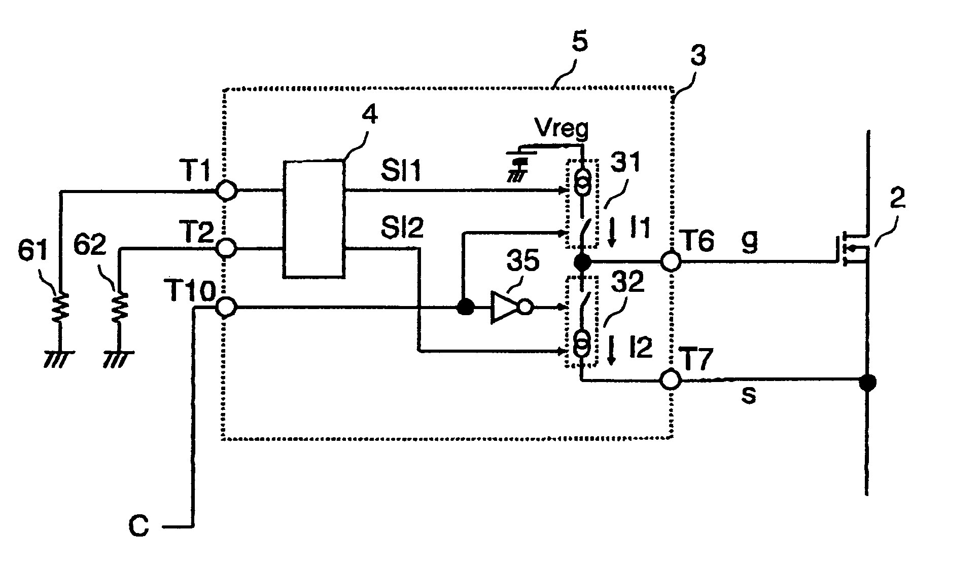
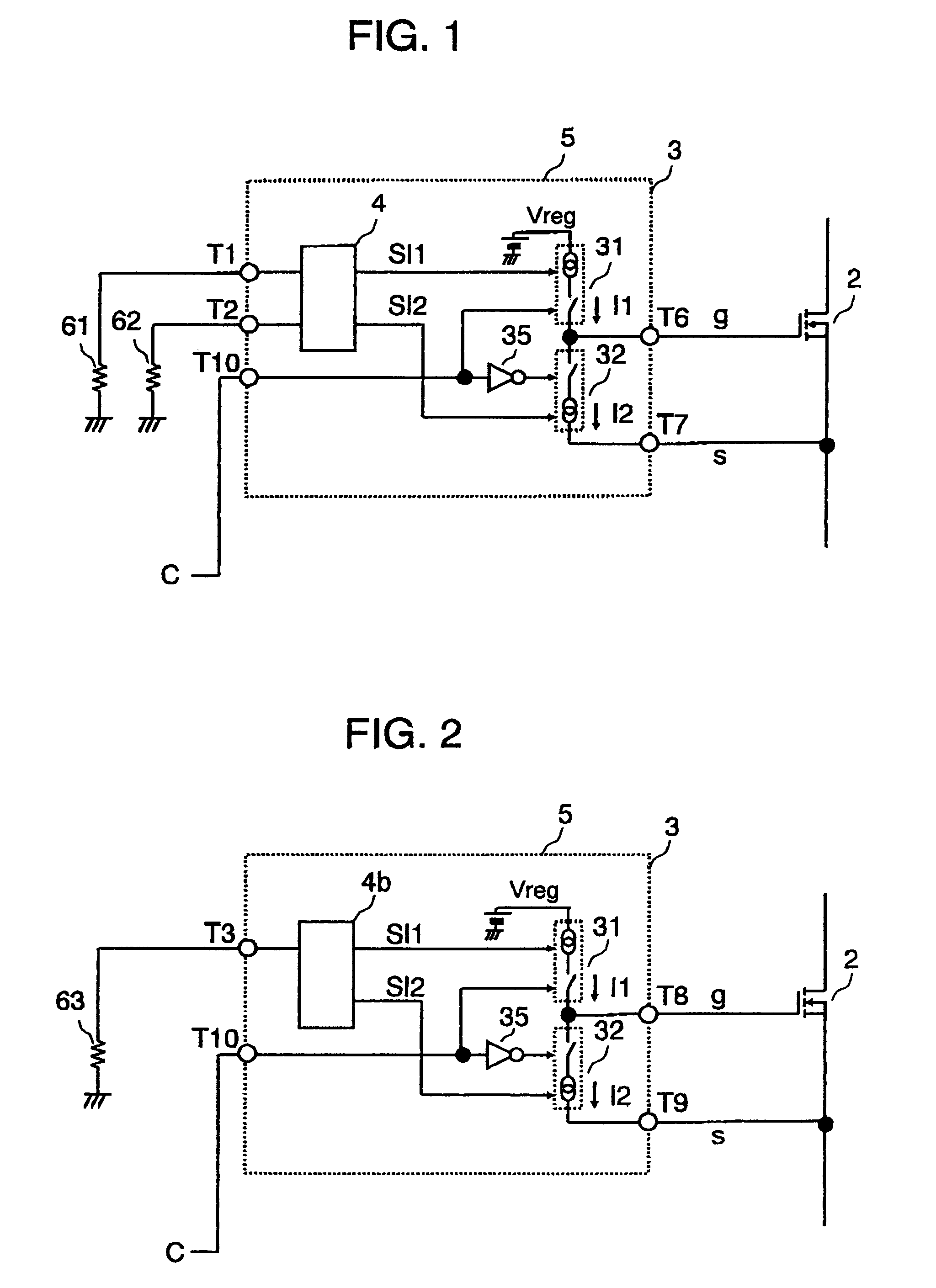
[0049]FIG. 1 shows a structure of a gate driver in accordance with the first exemplary embodiment of the present invention. In FIG. 1, power transistor 2 includes a gate electrode insulated with oxide film, and MOSFET or IGBT is well known as this type of power transistor. In the first embodiment, the MOSFET is used as an example.
[0050]Gate driver 3 has a coupler for connecting with the outside, and the coupler comprises the following elements:[0051]a connecting section with a gate electrode (terminal T6);[0052]a connecting section with a source electrode (terminal T7); and[0053]a cluster of input terminals that receives gate-driver control information (assigning terminal T1, assigning terminal T2, and an input terminal that receives switch control signal C (terminal T10)).
Gate driver 3 further includes the following elements as its interior structure:[0054]first current source 31;[0055]second current source 32;[0056]gate circuit (NOT circuit) 35; and[0057]current assignor 4.
[0058]S...
exemplary embodiment 2
[0079]FIG. 2 shows a structure of a gate driver in accordance with the second exemplary embodiment of the present invention. In the first embodiment discussed previously, resistors 61 and 62 are coupled to two assigning terminals T1 and T2, thereby assigning first current value I1 and second current value I2. In this second embodiment, gate driver 3 includes one assigning terminal T3 coupled with resistor 63 as shown in FIG. 2, so that current values I1 and I2 are assigned.
[0080]To be more specific, current assignor 4b has a predetermined ratio of current assigning signal SI1 vs. SI2. Based on a value of resistor 63 coupled to terminal T3, current assignor 4b outputs signals SI1 and SI2 in response to the foregoing ratio. Current value I1 in response to signal SI1 is supplied to a gate electrode of power transistor 2 via terminal T8. Current value I2 in response to signal SI2 is supplied to a source electrode of transistor 2 via terminal T9. Switch control signal C supplied to termi...
exemplary embodiment 3
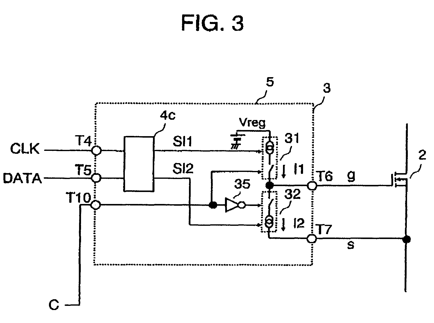
[0083]FIG. 3 shows a structure of a gate driver in accordance with the third exemplary embodiment of the present invention. In this third embodiment, for instance, terminals CLK and DATA, which receive communication information, can be used as assigning terminals T4 and T5 as shown in FIG. 3, and serial communication information is supplied to those terminals. Based on the serial communication information, current assignor 4c assigns current values I1 and I2. In FIG. 3, the input terminals CLK and DATA are used; however, there are various methods in the serial communications, for instance, only DATA terminal is prepared as an input terminal, or an enable terminal is added, so that this embodiment can be achieved in a variety of communication forms. Switch control signal C supplied to terminal 10 works in a similar manner to the first embodiment.
[0084]The third embodiment proves that a time needed to change a shut-off state of transistor 2 to a conductive state or vice versa can be p...
PUM
 Abstract
Description
Claims
Application Information


