Simulator for a chemical mechanical polishing

a mechanical polishing and simulation technology, applied in the field of simulations, can solve problems such as difficult to obtain a predetermined image forming performance, poor image forming performance, and substrate irregularities

Active Publication Date: 2008-04-22
RENESAS ELECTRONICS CORP
View PDF14 Cites 45 Cited by
  • Summary
  • Abstract
  • Description
  • Claims
  • Application Information

AI Technical Summary

Benefits of technology

[0015]It is an object of the present invention to provide a simulator that ca

Problems solved by technology

The circuit pattern is formed by the optical transfer method as described above, and a transfer in a defocus state produces a blurred image, resulting in poor image forming performance.
On the other hand, repetitive processes such as selective etching and film formation are executed on the semiconductor substrate, and irregularities

Method used


Image

  • Simulator for a chemical mechanical polishing
  • Simulator for a chemical mechanical polishing
  • Simulator for a chemical mechanical polishing

Examples


Embodiment Construction

Technical Idea of the Present Invention

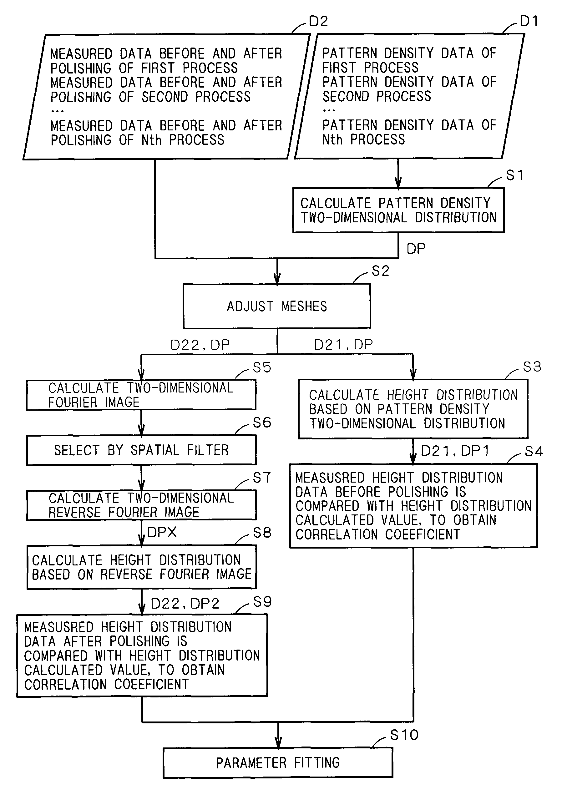
[0032]When manufacturing large scale integrated circuits (LSIs), a plurality of LSIs called “sub-chips,” including a TEG (test element group) and a process monitor, are also formed on a semiconductor substrate in addition to a target LSI called “main chip.” The plurality of sub-chips are formed in a region other than a region for forming the main chip.

[0033]Not only a circuit pattern of the main chip but also circuit patterns of the plurality of sub-chips are formed in a transfer mask used in the individual processes for forming the main chip and sub-chips on the semiconductor substrate.

[0034]To form the transfer mask, it is possible to use in the state that design data of the main chip and sub-chips are already synthesized. However, it is preferably split and processed because the actual LSI design data is tremendous. Therefore, the design data are often split in units of sub-chips and the split data are used sequentially.

[0035]Splitting desig...


PUM


Abstract

A simulator is provided which can simulate in consideration of various parameters in a CMP process. A pattern density two-dimensional distribution calculating part takes a pattern density two-dimensional distribution image. A mesh adjusting part performs a mesh adjustment of a measured data. A height distribution calculating part calculates a height distribution based on the pattern density two-dimensional distribution image. A correlation coefficient calculating part calculates a correlation coefficient by performing a least squares analysis of a measured data and a height distribution data. Passing through a Fourier calculation part, spatial filter part, and reverse Fourier calculating part, the pattern density two-dimensional distribution image becomes a pattern density two-dimensional distribution image. This distribution image further passes through a height distribution calculating part, resulting in a height distribution data. The correlation coefficient calculating part calculates a correlation coefficient by performing a least squares analysis of the height distribution data and measured data after CMP process.

Description

BACKGROUND OF THE INVENTION[0001]1. Field of the Invention[0002]The present invention relates to a simulator, and more particularly to a simulator for a chemical mechanical polishing (CMP) process used in the manufacture of semiconductor devices.[0003]2. Description of the Background Art[0004]The miniaturization and high integration of large scale integrated circuits (LSIs) creates the tendency that circuit patterns formed on the LSIs have a minimum pattern dimension of 0.1 μm. A circuit pattern of an LSI can be formed in a manner that writes a design circuit on a transfer mask for implementing it on a semiconductor substrate by laser or electron beam, and then performs a batch optical transfer of the transfer mask pattern onto the semiconductor substrate by a projection transfer apparatus.[0005]The resolution R of the transfer apparatus is given by the following expression:R=k1λ / NA[0006]where k1 represents a process constant, λ represents a waveform, and NA represents a numerical a...

Claims


Application Information

Patent Timeline
IPC IPC(8): G06F17/50H01L21/304G06F17/10H01L21/00H01L21/302H01L21/306H01L21/66
CPCB24B37/042G06F17/5022H01L21/67253G06F2217/12G06F30/33G06F2119/18Y02P90/02H01L21/304
Inventor KAMON, KAZUYA
Owner RENESAS ELECTRONICS CORP
Why Eureka
Try Eureka