Sensor semiconductor device with sensor chip

a technology of semiconductor devices and sensors, applied in the direction of semiconductor devices, basic electric elements, electrical equipment, etc., can solve the problems of large increase in fabrication costs, circuit cracking, and failure of electrical connections, and achieve the effects of reducing stress concentration effects, and reducing the overall thickness of fabricated semiconductor devices

Inactive Publication Date: 2008-04-29
SILICONWARE PRECISION IND CO LTD
View PDF3 Cites 9 Cited by
  • Summary
  • Abstract
  • Description
  • Claims
  • Application Information

AI Technical Summary

Benefits of technology

[0007]In light of the above drawbacks in the conventional technology, an objective of the present invention is to provide a sensor semiconductor device and a method for fabricating the same, whereby the sensor semiconductor device can be easily fabricated.
[0009]Still another objective of the present invention is to provide a sensor semiconductor device and a method for fabricating the same, whereby a circuit-cracking problem is avoided.
[0013]By the sensor semiconductor device and the method for fabricating the same in the present invention, a sensor chip is firstly mounted on a substrate, and then a dielectric layer and a circuit layer are formed on the substrate by a build-up process. The circuit layer is electrically connected to the substrate and the sensor chip, such that the sensor chip can be electrically connected to the substrate via the circuit layer. The dielectric layer is formed with an opening for exposing a sensor region of the sensor chip. A light-penetrable lid is provided to cover the opening of the dielectric layer, such that light is able to penetrate the light-penetrable lid to reach the sensor region and activate the sensor chip. A plurality of solder balls are implanted on a surface of the substrate not for mounting the sensor chip, so as to allow the sensor chip to be electrically connected to an external device by the solder balls. In the present invention, the sensor chip can be subjected to a test and any defective chip failing in the test is eliminated in advance, such that the reliability of subsequent fabricating processes is improved and a known good die (KGD) problem is avoided. The sensor chip can be thinned before being mounted on the substrate, such that an overall thickness of the fabricated semiconductor device is reduced. A chamfer can be formed on the active surface of the sensor chip by bevel cutting so as to reduce a stress concentration effect. By the arrangement that the sensor chip is electrically connected to the substrate via the circuit layer through the build-up process, and the sensor chip is electrically connected to the solder balls via circuits and conductive vias of the substrate and is further electrically connected to the external device via the solder balls, the sensor semiconductor device can be fabricated in an easy and cost-effective manner as compared to the conventional technology, and a chip-cracking problem is prevented in the present invention.

Problems solved by technology

However, in the foregoing sensor semiconductor device, since the circuit layers formed on the side walls of the inclined slots have an acute angle relative to the electrode pads of the sensor chip electrically connected to the circuit layers, such acute-angle connection positions between the circuit layers and the electrode pads may easily be subject to stress concentration, thereby causing problems such as circuit cracking, failure in electrical connection, and so on.
As fabrication of the foregoing sensor semiconductor device is directly performed on the wafer, which requires complicated fabrication processes and does not effectively solve a known good die (KGD) problem, making the fabrication costs greatly increased.

Method used


Image

  • Sensor semiconductor device with sensor chip
  • Sensor semiconductor device with sensor chip
  • Sensor semiconductor device with sensor chip

Examples


Embodiment Construction

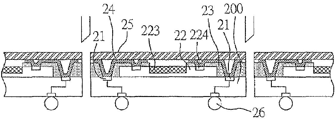
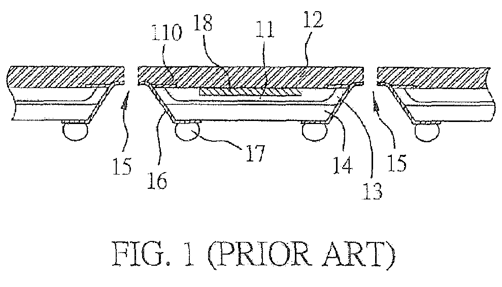
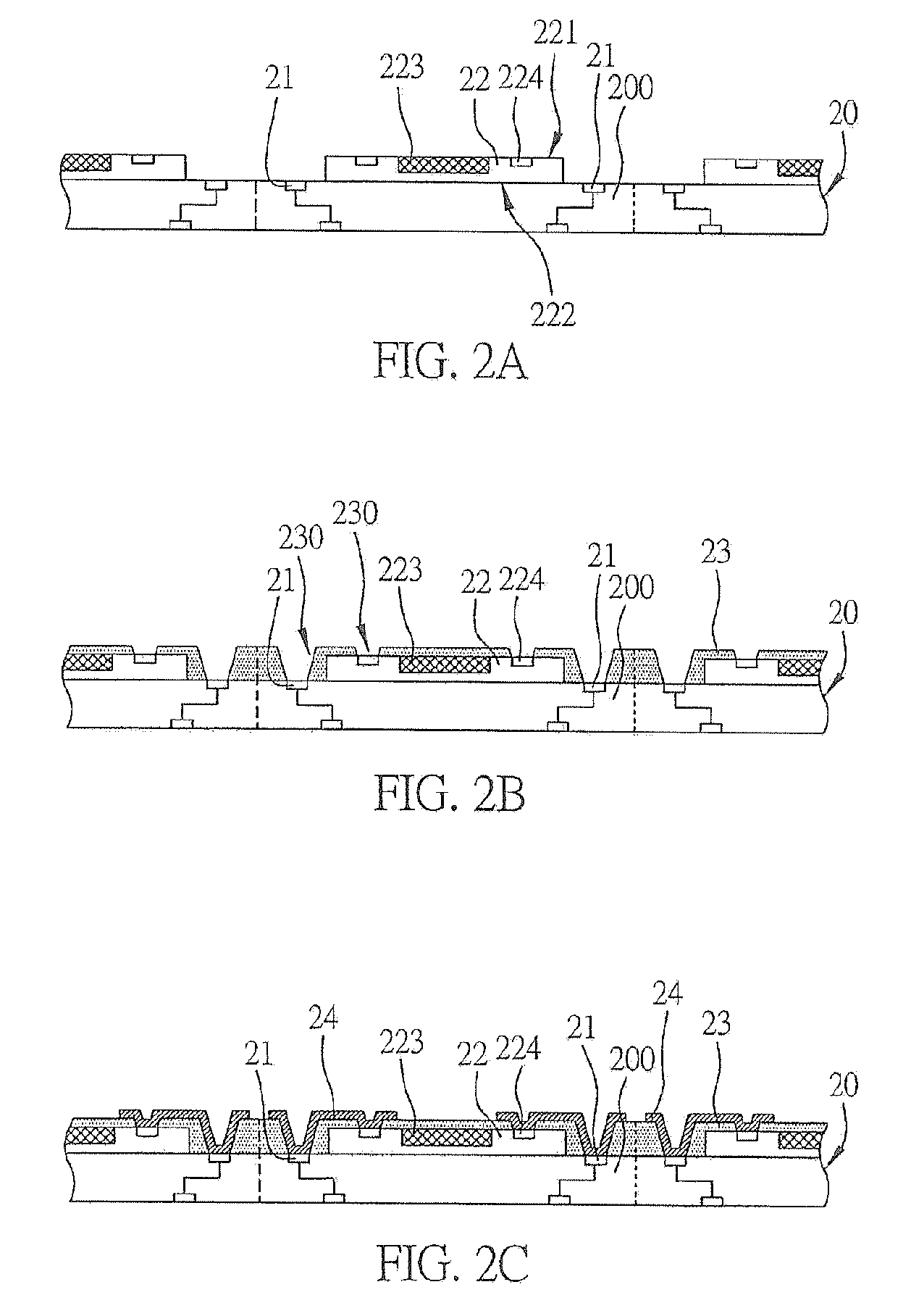
[0019]Preferred embodiments of a sensor semiconductor device and a method for fabricating the same proposed in the present invention are described below with reference to FIGS. 2A-2E, 3 and 4. It should be noted that the drawings are simplified schematic diagrams for illustrating the basic design of the present invention and thus only show relevant elements to the present invention. The drawings are not made with the actual amount, shape and size of the elements. In practice, the number, shape and size of the elements can be flexibly modified, and an element layout may be more complex.

[0020]FIGS. 2A to 2E are cross-sectional views of steps of a method for fabricating a sensor semiconductor device according to a first preferred embodiment of the present invention. In this embodiment, a batch-type method is employed to fabricate the sensor semiconductor device. It should be understood that the sensor semiconductor device in the present invention can also be fabricated in a singular-ty...


PUM


Abstract

A sensor semiconductor device and a method for fabricating the same are proposed. A sensor chip is mounted on a substrate, and a dielectric layer and a circuit layer are formed on the substrate, wherein the circuit layer is electrically connected to the substrate and the sensor chip. The dielectric layer is formed with an opening for exposing a sensor region of the sensor chip. A light-penetrable lid covers the opening of the dielectric layer, such that light is able to penetrate the light-penetrable lid to reach the sensor region and activate the sensor chip. The sensor chip can be electrically connected to an external device via a plurality of solder balls implanted on a surface of the substrate not for mounting the sensor chip. Therefore, the sensor semiconductor device is fabricated in a cost-effective manner, and circuit cracking and a know good die (KGD) problem are prevented.

Description

FIELD OF THE INVENTION[0001]The present invention relates to sensor semiconductor devices and methods for fabricating the same, and more particularly, to a chip-scale packaged (CSP) sensor semiconductor device, and a method for fabricating the sensor semiconductor device.BACKGROUND OF THE INVENTION[0002]In a conventional image sensor package, a sensor chip is mounted on a chip carrier and is electrically connected to the chip carrier via bonding wires, and a piece of glass is provided above the sensor chip to allow an image to be captured by the sensor chip. The image sensor package can be integrated to an external device such as a printed circuit board (PCB) to be used in various electronic products such as digital still camera (DSC), digital video camera (DVC), optical mouse, cellular phone, fingerprint scanner, and so on.[0003]Along with expansion of data transmission capacity and development of miniaturized and portable electronic products, integrated circuit (IC) packages have ...

Claims


Application Information

Patent Timeline
Patent Type & Authority Patents(United States)
IPC IPC(8): H01L29/267H01L29/22
CPCH01L27/14618H01L27/14683H01L2224/24226
Inventor HUANG, CHIEN-PINGHUANG, CHIH-MINGCHANG, CHENG-YI
Owner SILICONWARE PRECISION IND CO LTD
Why Eureka
Try Eureka