Resistive elements using carbon nanotubes

a technology of carbon nanotubes and resistive elements, applied in the field of thin film resistors, can solve the problems of difficult design and fabrication, and large resistance values in excess of 100 k-ohms, and achieve the effects of improving parameter control, increasing the function per device, and prolonging the battery li

Active Publication Date: 2008-04-29
NANTERO
View PDF30 Cites 65 Cited by
  • Summary
  • Abstract
  • Description
  • Claims
  • Application Information

AI Technical Summary

Benefits of technology

[0014]The present invention provides resistive elements using carbon nanotubes. The inventors have appreciated that carbon nanotubes can be used in miniaturized low-TCR resistive elements having improved parameter control and associated increased function per device. They may be used, for example, to extend battery life, improve signal integrity, offer performance gains and other advantages depending on the application. By using high-ohm miniature resistors with low-current consumption, extended battery life may be achieved in medical applications such as implantable and portable devices that rely on extended battery life. Military requirements for miniaturized portable next generation radio, GPS, and command-and-control systems also may use thin film resistors to improve signal integrity and maximize system performance (per send-and-receive watts) by maximizing battery life. Test-and-measurement devices now require speeds in excess of 100 GHz and require miniature thin film resistors with low parasitic capacitance and inductance values to achieve reproducible test results.
[0015]Under one aspect of the invention, a resistive element includes a patterned region of nanofabric with predefined area, the nanofabric having a selected sheet resistance. First and second electrical contacts contacting the patterned region of nanofabric and in spaced relation to each other. The resistance of the element between the first and second electrical contacts is determined by the selected sheet resistance of the nanofabric and the predetermined area and the spaced relation of the first and second electrical contacts. The bulk resistance of the element is tunable.

Problems solved by technology

Some presently available high performance thin-film resistors are capable of exhibiting low TCRs, but their applicability is limited because they are not able to carry large currents.
Large resistance values in excess of 100 K-Ohms are difficult to design are difficult to design and fabricate.

Method used


Image

  • Resistive elements using carbon nanotubes
  • Resistive elements using carbon nanotubes
  • Resistive elements using carbon nanotubes

Examples


example 1

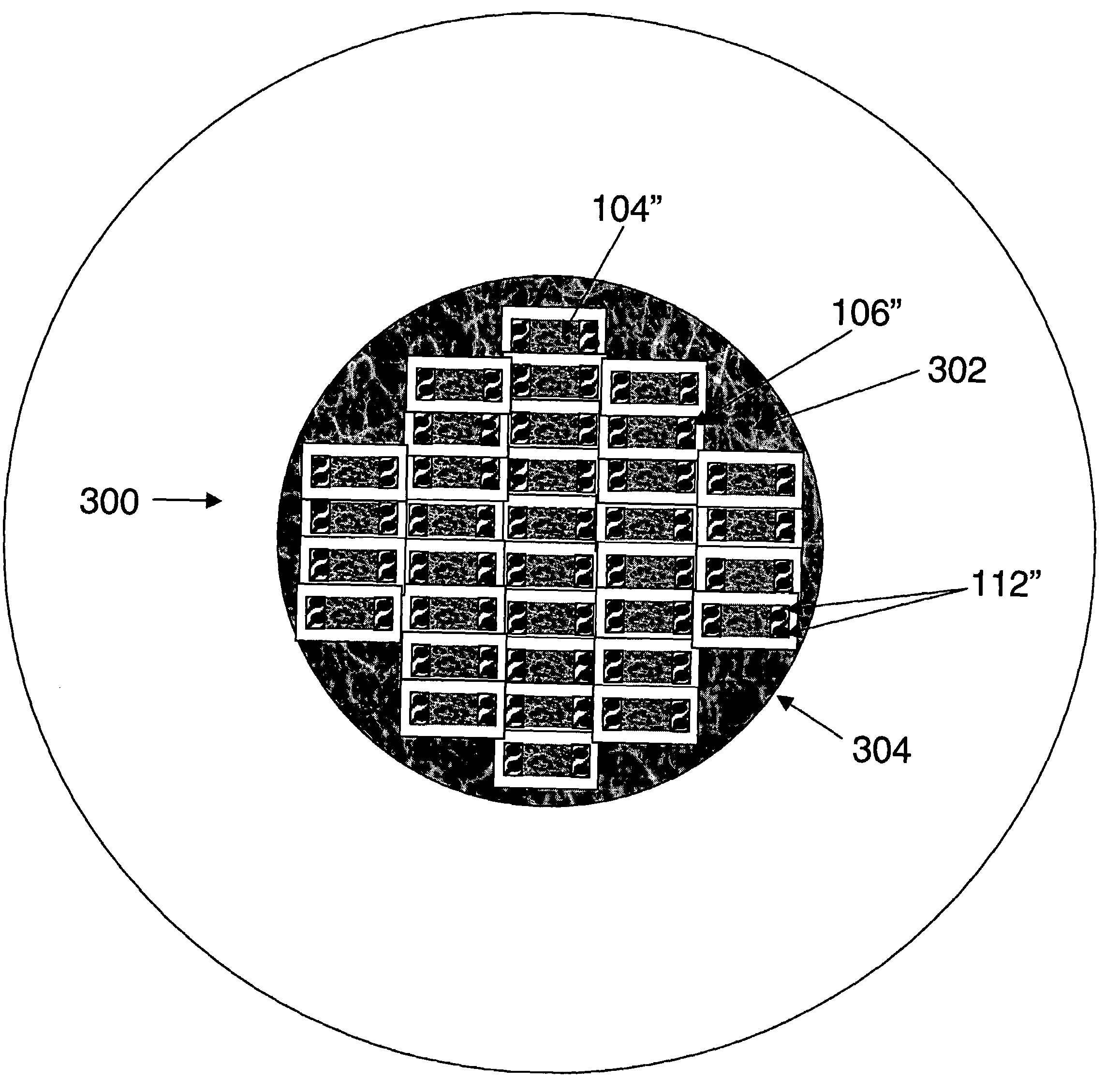
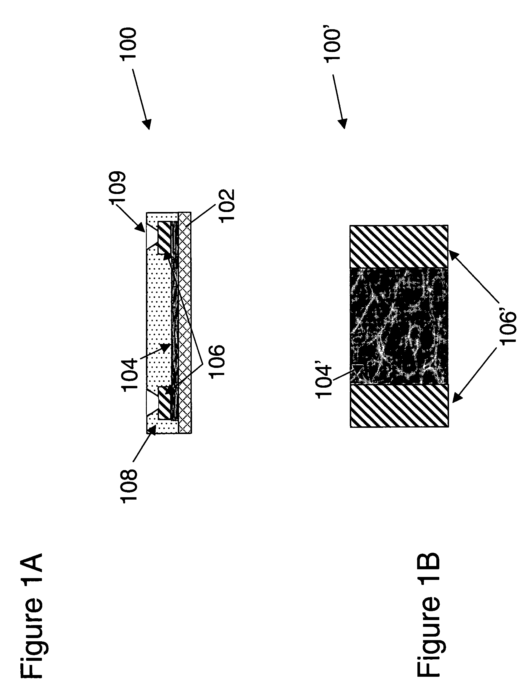
[0041]FIG. 3B illustrates 31 different four-point probe locations 312 on wafer substrate 304 for probing the sheet resistance of nanofabric layer 302 (layer 302 is shown in FIG. 3A) prior to nanotube resistive element patterning. Preferred methods deposit nanofabric layer 302 by spinning an electronic-grade carbon nanotube solution, which includes electronic-grade nanotubes suspended in a coating track-compatible solvent, in a semiconductor fabricator. Thus, nanofabric layer 302 is deposited on a wafer 304 in a semiconductor fabricator using techniques compatible with semiconductor processes (see, e.g., incorporated patent references). Preferred methods include removing the nanotube fabric edge bead. Although patterned nanotube resistive elements are shown as discrete resistors, patterned resistive elements may also be integrated with integrated circuits. Nanofabric layer 302 is a conformal monolayer approximately 1.5 nm thick and may be introduced at any process level after formati...

example 2

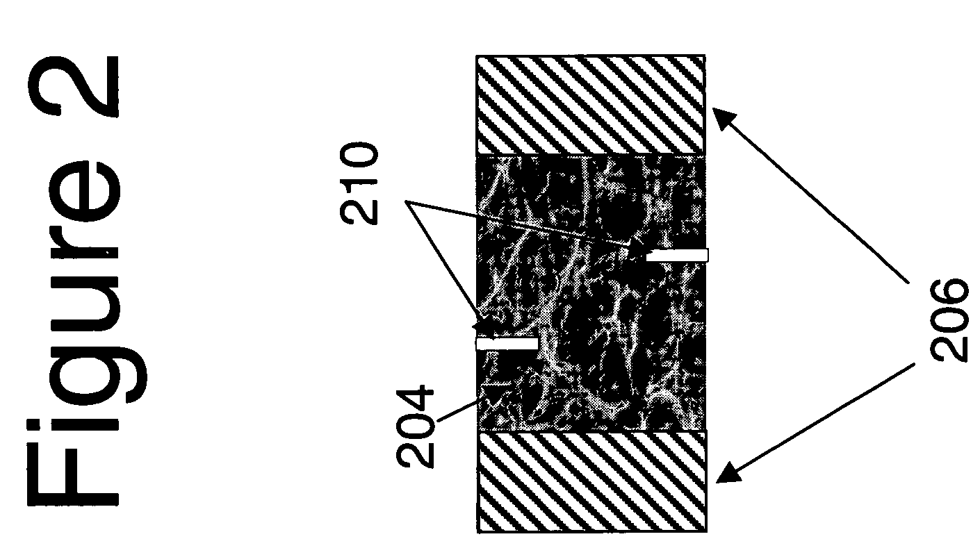
[0051]A nanofabric layer (nanofabric) was produced and reliably reproduced having a sheet resistance of 65 K-Ohms-per-square. Resistances were measured at temperatures ranging from −40 degrees C. to 140 degrees C. in air. A four-point probe was used (Os tips, at 0.04 inch spacing, each probe had a 0.01 inch radius, 45 grams of pressure applied and 300 uAmps of current). The investigators calculated a TCR for the film of −22 ppm resistance change per degree, as shown in FIG. 5, which is a graph 500 of ambient temperature vs. Kilo-Ohms resistance in the fabric. This measurement was found to be reliably reproducible, and associated electron transport was hypothesized to be quasiballistic. In the case of the 5 M-Ohm resistor design described in example 1, for a sheet resistance of 60 K-Ohms-per-square, resistive element 100 (as shown in FIG. 1A) requires 77 squares between contacts, corresponding to 154 um of length, and also 2 um of width. As previously described, contact resistances a...


PUM

PropertyMeasurementUnit
temperaturesaaaaaaaaaa
thicknessaaaaaaaaaa
thicknessaaaaaaaaaa

Abstract

Resistive elements include a patterned region of nanofabric having a predetermined area, where the nanofabric has a selected sheet resistance; and first and second electrical contacts contacting the patterned region of nanofabric and in spaced relation to each other. The resistance of the element between the first and second electrical contacts is determined by the selected sheet resistance of the nanofabric, the area of nanofabric, and the spaced relation of the first and second electrical contacts. The bulk resistance is tunable.

Description

CROSS-REFERENCE TO RELATED APPLICATIONS[0001]This application claims priority under 35 U.S.C. §119(e) to the following application, the contents of which are incorporated herein in their entirety by reference:[0002]U.S. Provisional Patent Application No. 60 / 611,765, filed on Sep. 21, 2004, entitled Resistive Elements Using Carbon Nanotubes.BACKGROUND[0003]1. Technical Field[0004]The present application relates generally to the field of thin film resistors, both in integrated circuits and as discrete resistors, more specifically to thin film resistors with improved temperature independence, and even more specifically to thin film resistors fabricated from carbon nanotube fabrics.[0005]2. Discussion of Related Art[0006]Thin film resistors are used in many important technological applications as parts of electronic circuits. Thin film resistors may be integrated into complex hybrid circuitry, and / or they may be used as discrete devices. For example, thin film resistors can be used in i...

Claims


Application Information

Patent Timeline
Patent Type & Authority Patents(United States)
IPC IPC(8): H01C10/00
CPCH01C7/005H01C7/06H01C10/306H01C17/0652H01C17/232H01L28/22H01C7/003H01C7/006H01C17/283
Inventor BERTIN, CLAUDE L.RUCKES, THOMASSEGAL, BRENT M.WARD, JONATHAN W.
Owner NANTERO
Why Eureka
Try Eureka