Evaluation method of fine pattern feature, its equipment, and method of semiconductor device fabrication

a technology of fine pattern and equipment, which is applied in the direction of semiconductor/solid-state device testing/measurement, mechanical roughness/irregularity measurement, instruments, etc., can solve the problems of small deviations from the design value of the pattern, the average gate length of the transistor itself deviating from the design value, and the transistor performance getting worse than the design value. , to achieve the effect of easy adjustment of setting, easy adjustment of transistor performance distribution, and high reliability

Active Publication Date: 2008-04-29
HITACHI HIGH-TECH CORP
View PDF5 Cites 28 Cited by
  • Summary
  • Abstract
  • Description
  • Claims
  • Application Information

AI Technical Summary

Benefits of technology

[0034]If such a method is used, it is possible to quickly obtain the components of roughness in an arbitrary frequency region band being set up in advance without the necessity of determination of the operator and save the results so that the results can be checked later.
[0050]The evaluation method of fine pattern feature and its equipment according to this invention enable a frequency component causing important influence, especially in device performance, among frequency components of line-edge roughness to be extracted and expressed in a numerical term. Since the frequency band of a component affecting the device performance depends on a device structure and final specifications of a product, setting must be altered easily by the equipment operator. This invention allows for the operator to alter setting, and therefore can realize order-made inspection suited to a product, increasing productivity.

Problems solved by technology

Recently, with improvement in fine pattern processing technologies in semiconductor and other industries, small deviations from design values of the pattern become problems.
Especially, degradation in a two-dimensional form and dimensional variation that are noticeable even by top-down observation cause large influence in device performance.
Therefore, even if the average gate length in the transistor has such a value as a design specifies, transistor performance gets worse than a design value.
Second, the average gate length in the transistor itself deviates from the design value.
As a result, a problem of measurement of line-edge roughness in addition to the conventional dimensional measurement has arisen also in measurement equipment.
However, determination using one kind of index out of these indexes has two problems.
First, this determination cannot compare data of different sampling conditions.
For example, in the case where two kinds of patterns A and B are measured with respective different observation magnifications, it is very difficult to equalize a detection interval of edge-points used to calculate line-edge roughness and a measurement area for two kinds of images, because the length and resolution for one pixel are different.
Such a problem is likely to occur in a research and development phase.
Second, a spatial period of roughness cannot be expressed with one kind of index.
In a process of making transistors of short gate widths, roughness of a long period becomes comparatively large.
However, it is difficult to grasp instantaneously characteristics of the line-edge roughness related to the frequency distribution visually from these spectra on which noises have a large influence.
Because of this, measured values of CD uniformity across a wafer plane and amount of variation among wafers depend on line-edge roughness occurring at random, and consequently it becomes impossible to measure CD variation resulting from variation in anneal temperature and variation in an underlayer thickness.

Method used


Image

  • Evaluation method of fine pattern feature, its equipment, and method of semiconductor device fabrication
  • Evaluation method of fine pattern feature, its equipment, and method of semiconductor device fabrication
  • Evaluation method of fine pattern feature, its equipment, and method of semiconductor device fabrication

Examples


first embodiment

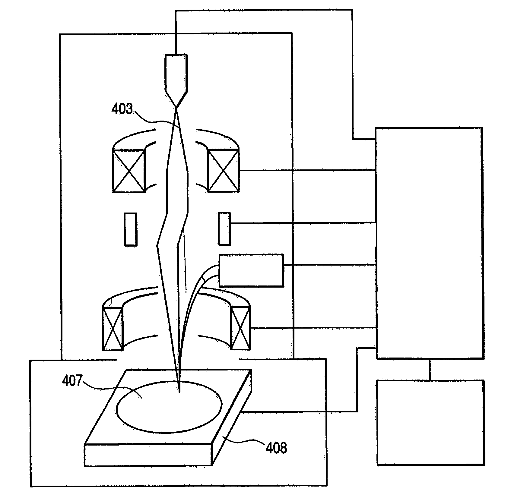
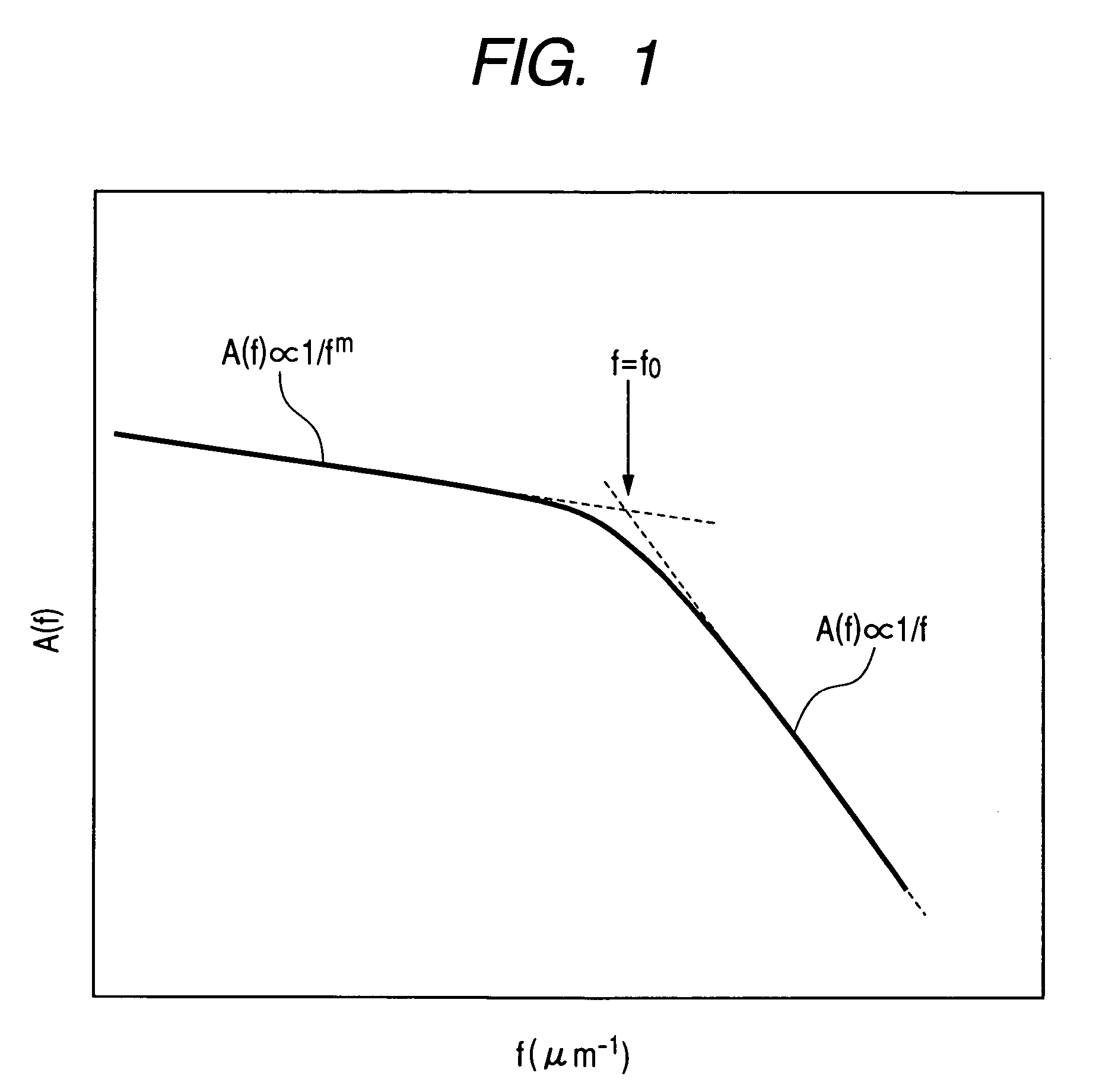
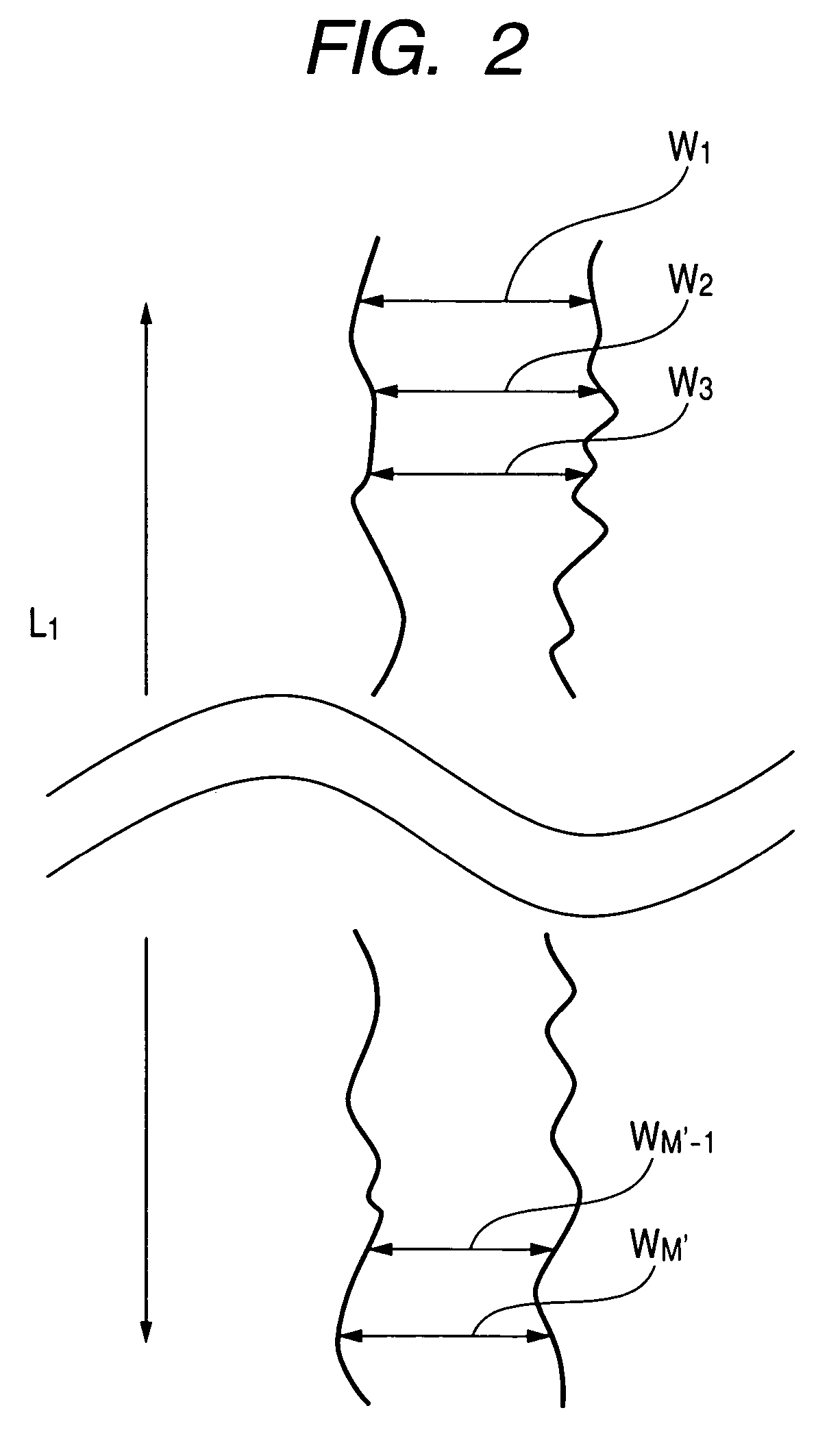
[0066]A first embodiment of this invention will be described using FIG. 4 to FIG. 9. FIG. 4 is a schematic diagram showing a structure of inspection equipment used in this embodiment, FIG. 5 is a schematic diagram showing a position of an inspected chip on a wafer in this embodiment, FIG. 6 is a flowchart showing a part of a procedure of analyzing a two-dimensional signal intensity distribution obtained by observation, FIG. 7 is a Fourier spectrum displayed on a display of the inspection equipment, FIG. 8 is a window used for specifying by inputs a region where measurement results of the roughness data are Fourier transformed and absolute values of the Fourier coefficients squared are integrated, and FIG. 9 is a diagram showing an integration region displayed on the spectrum shown in FIG. 7 and a roughness index 3σc obtained from an integration value of the power spectrum σc2, which are evaluation results displayed on the display of the inspection equipment when analysis of one line...

second embodiment

[0084]A second embodiment of this invention will be described using FIG. 4 and FIG. 10. FIG. 4 is a schematic diagram showing a structure of the inspection equipment that was used in this embodiment. FIG. 10 is a flowchart showing a part of procedure for analyzing a two-dimensional signal intensity distribution obtained in this embodiment as a result of observation.

[0085]This embodiment shows an example where inspection that uses the equipment of this invention is performed in an inspection process at the time of semiconductor device production, and the yield of manufacture is improved by monitoring the short-period roughness besides the long-period roughness.

[0086]In the semiconductor manufacturing process described in this embodiment, transistors of gate widths wg of about 300 nm were mainly made, and there was a possibility that performance variation in a transistor by the roughness whose spatial period is longer than 300 nm might cause a yield drop. At the same time, there was f...

third embodiment

[0099]A third embodiment of this invention will be described using FIG. 6, FIG. 11, and FIG. 12. FIG. 6 is a flowchart showing a part of a procedure of analyzing an electron microscope observation image in this embodiment, FIG. 11 shows a pattern under a resist film 1101 of a sample 1102 inspected in this embodiment, and FIG. 12 is an example of a resist pattern inspected in this embodiment.

[0100]This embodiment shows an example where inspection using the equipment of this invention is performed in an inspection process at the time of semiconductor device production and a variation in a line width that has a specific frequency is monitored, whereby the yield of manufacture is improved.

[0101]In the semiconductor manufacturing process described in this embodiment, prior to steps in which a layer of important line pattern is processed, a line pattern of a metal material running in a direction perpendicular to a line for gate was formed as shown in FIG. 11. An insulating material is dep...


PUM


Abstract

Equipment extracts components of spatial frequency that need to be evaluated in manufacturing a device or in analyzing a material or process out of edge roughness on fine line patterns and displays them as indexes. The equipment acquires data of edge roughness over a sufficiently long area, integrates a components corresponding to a spatial frequency region being set on a power spectrum by the operator, and displays them on a length measuring SEM. Alternatively, the equipment divides the edge roughness data of the sufficiently long area, computes long-period roughness and short-period roughness that correspond to an arbitrary inspection area by performing statistical processing and fitting based on theoretical calculation, and displays them on the length measuring SEM.

Description

CLAIM OF PRIORITY[0001]The present application claims priority from Japanese application JP 2004-22737 filed on Jul. 30, 2004, the content of which is hereby incorporated by reference into this application.FIELD OF THE INVENTION[0002]The present invention relates to an evaluation method of fine pattern feature by detailed feature metrology by means of non-destructive observation with a scanning electron microscope (SEM) and image processing or by dimensional measurement, its inspection equipment, and a method of semiconductor device manufacture.BACKGROUND OF THE INVENTION[0003]Recently, with improvement in fine pattern processing technologies in semiconductor and other industries, small deviations from design values of the pattern become problems. Especially, degradation in a two-dimensional form and dimensional variation that are noticeable even by top-down observation cause large influence in device performance. Then, there has arisen a need to measure and evaluate edge roughness ...

Claims


Application Information

Patent Timeline
Patent Type & Authority Patents(United States)
IPC IPC(8): G06F19/00G01B15/04H01L21/66
CPCG01B15/08G01N23/2251G03F7/70625H01J2237/223H01J2237/2817
Inventor YAMAGUCHI, ATSUKOFUKUDA, HIROSHIKAWADA, HIROKIMAEDA, TATSUYA
Owner HITACHI HIGH-TECH CORP
Why Eureka
Try Eureka