Accumulation device with charge balance structure and method of forming the same

a technology of accumulation mode and charge balance, which is applied in the direction of dc-ac conversion without reversal, transistors, basic electric elements, etc., can solve the problems of low efficiency and low on-resistance, and achieve the effect of increasing the blocking capability of accumulation-mode field effect transistors

Active Publication Date: 2008-05-06
SEMICON COMPONENTS IND LLC
View PDF364 Cites 50 Cited by
  • Summary
  • Abstract
  • Description
  • Claims
  • Application Information

AI Technical Summary

Benefits of technology

[0006]In accordance with an embodiment of the present invention, an accumulation-mode field effect transistor includes a plurality of gates and a semiconductor region having a channel region adjacent to but insulated from each of the plurality of gates. The semiconductor region further includes a conduction region wherein the channel regions and the conduction region are of a first conductivity type. The transistor further includes a drain terminal and a source terminal configured so that when the accumulation-mode field effect transistor is in the on state a current flows from the drain terminal to the source terminal through the conduction region and the channel regions. A number of charge balancing structures are integrated with the semiconductor region so as to extend parallel to the current flow. In a blocking state, the charge balancing structures influence an electric field in the conduction region so as to increase the blocking capability of the accumulation-mode field effect transistor.

Problems solved by technology

A drawback of accumulation transistor 100 is that drift region 106 needs to be lightly doped to support a high enough reverse bias voltage.
However, a lightly doped drift region results in a lower on-resistance and lower efficiency.

Method used


Image

  • Accumulation device with charge balance structure and method of forming the same
  • Accumulation device with charge balance structure and method of forming the same
  • Accumulation device with charge balance structure and method of forming the same

Examples


Embodiment Construction

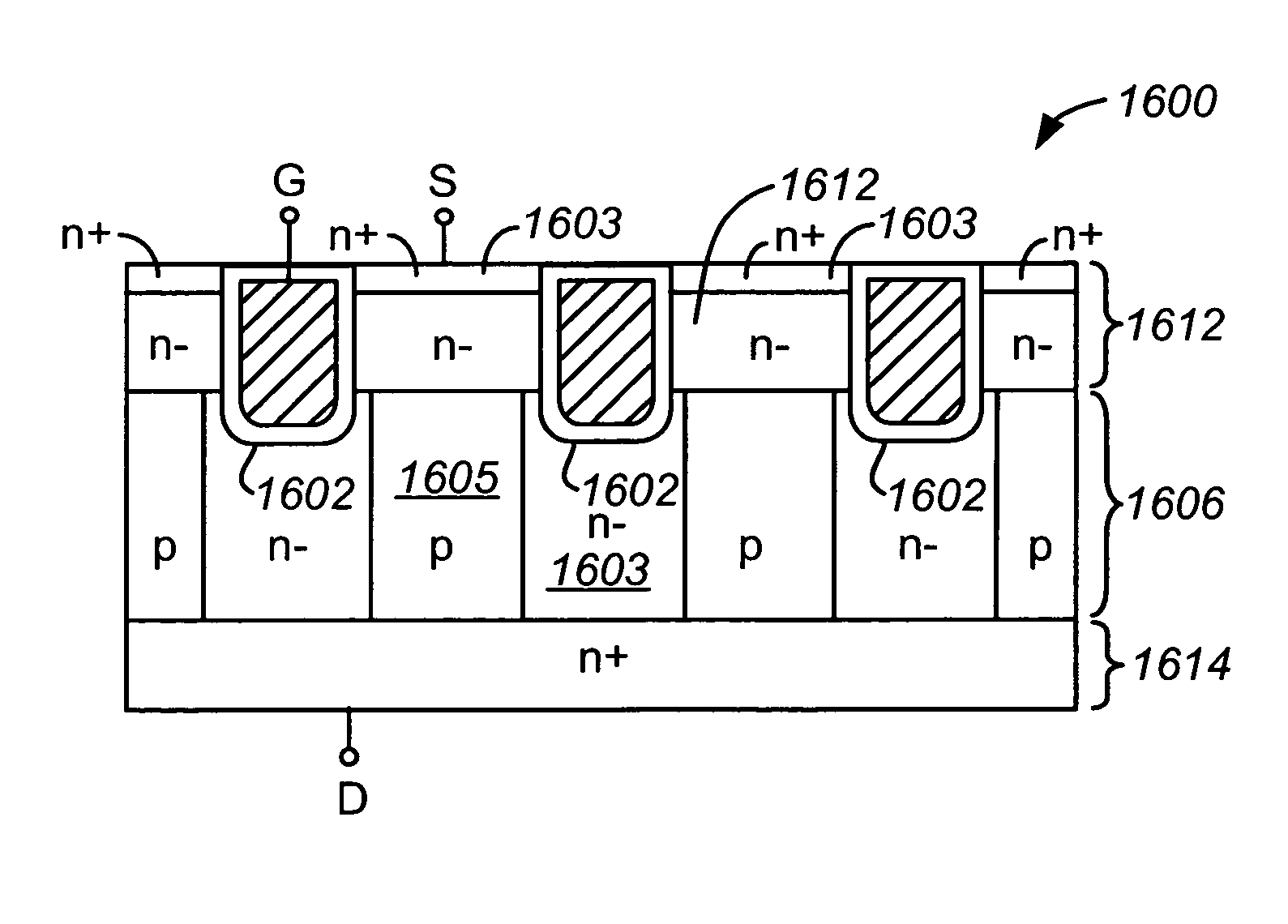
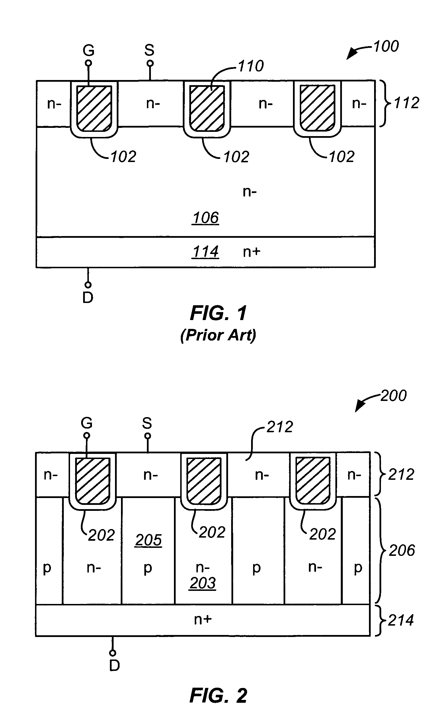
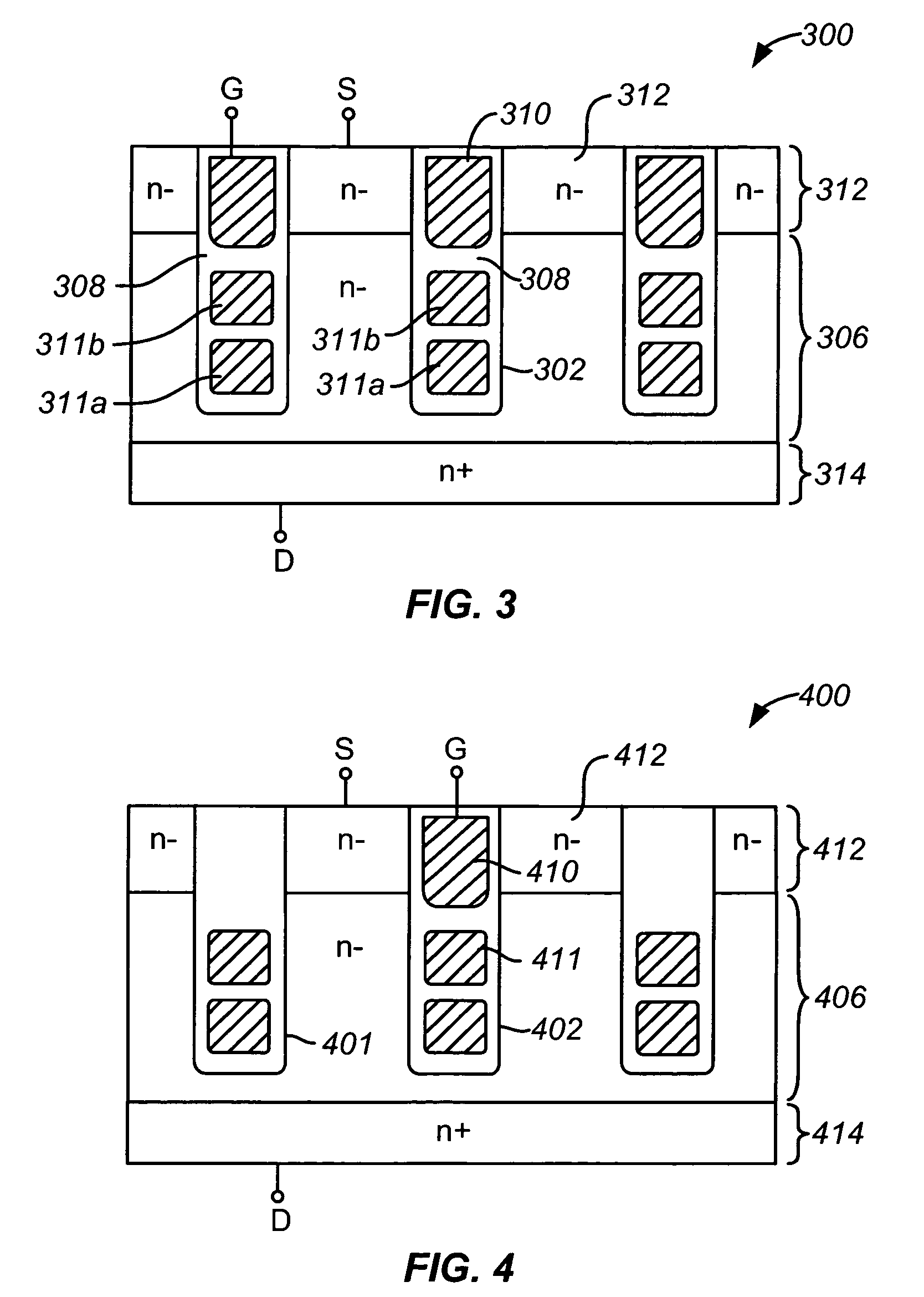
[0041]In accordance with the present invention, charge spreading techniques are advantageously integrated in vertical and lateral accumulation-mode power devices to achieve lower on-resistance, higher blocking capability and improved efficiency.

[0042]FIG. 2 shows a simplified cross section view of an exemplary accumulation-mode field effect transistor 200 with alternate conductivity regions 203, 205 extending vertically parallel to the current flow. In this example, transistor 200 is an n-channel transistor with a gate terminal formed inside each of trenches 202, n-type channel regions 212 between trenches 202, a drift region 206 that includes opposite polarity columnar n-type and p-type sections 203 and 205, and an n-type drain region 214. Unlike enhancement-mode transistors, accumulation-mode transistor 200 does not include a blocking (p-type in this example) well or body region inside which the conduction channel is formed. Instead a conducting channel is formed when an accumulat...


PUM


Abstract

An accumulation-mode field effect transistor includes a plurality of gates and a semiconductor region having a channel region adjacent to but insulated from each of the plurality of gates. The semiconductor region further includes a conduction region wherein the channel regions and the conduction region are of a first conductivity type. The transistor further includes a drain terminal and a source terminal configured so that when the accumulation-mode field effect transistor is in the on state a current flows from the drain terminal to the source terminal through the conduction region and the channel regions. A number of charge balancing structures are integrated with the semiconductor region so as to extend parallel to the current flow. In a blocking state, the charge balancing structures influence an electric field in the conduction region so as to increase the blocking capability of the accumulation-mode field effect transistor.

Description

CROSS-REFERENCES TO RELATED APPLICATIONS[0001]This application claims the benefit of U.S. Provisional Application No. 60 / 588,845, filed Jul. 15, 2004, and U.S. Provisional Application No. 60 / 669,063, filed Apr. 6, 2005, which are commonly assigned and incorporated herein by reference in their entirety for all purposes. Also, this application is a Continuation-In-Part of U.S. patent application Ser. No. 11 / 026,276, filed Dec. 29, 2004, which is commonly assigned and incorporated herein by reference in its entirety for all purposes.[0002]Further, this application is related to U.S. patent application Ser. No. 10 / 821,796, filed Apr. 9, 2004, U.S. patent application Ser. No. 10 / 288,982, filed Nov. 5, 2002, U.S. patent application Ser. No. 10 / 666,034, filed Sep. 18, 2003, and U.S. Pat. No. 6,376,878, issued on Apr. 23, 2002, all of which are incorporated herein by reference in their entirety for all purposes.BACKGROUND OF THE INVENTION[0003]The present invention relates in general to the...

Claims


Application Information

Patent Timeline
Patent Type & Authority Patents(United States)
IPC IPC(8): H01L27/108H01L29/76
CPCH01L21/3065H01L21/30655H01L21/31116H01L21/6835H01L21/823487H01L29/0623H01L29/0634H01L29/0696H01L29/1095H01L29/402H01L29/404H01L29/407H01L29/66734H01L29/7802H01L29/7804H01L29/7805H01L29/7806H01L29/7811H01L29/7813H01L29/7815H01L29/7828H01L29/7838H01L21/26586H01L2924/1305H01L2924/12032H01L2924/13091H01L23/4952H01L23/49816H01L29/0649H01L29/0653H01L29/165H01L29/41766H01L29/42368H01L29/4238H01L29/4933H01L29/495H01L29/7831H01L2221/6834H01L2221/68363H01L2224/16H01L2924/01012H01L2924/01078H01L2924/15311H01L2924/1532H01L2924/19041H01L2924/30105H01L2924/3011H01L2924/3025H02M3/00H02M3/33592H02M7/48Y02B70/1475H01L2924/00Y02B70/10H02M3/003
Inventor KOCON, CHRISTOPHER BOGUSLAW
Owner SEMICON COMPONENTS IND LLC
Why Eureka
Try Eureka