Differential amplifier and data driver employing the differential amplifier

a technology of differential amplifier and data driver, which is applied in the direction of pulse manipulation, pulse technique, instruments, etc., can solve the problems of increasing the chip area of the data driver lsi and to increase the cost, and reducing the circuit scale of the decoder. , to achieve the effect of saving the data drive area, reducing the number of gray level voltages, and reducing the number of gray level voltag

Inactive Publication Date: 2008-05-06
RENESAS ELECTRONICS CORP +1
View PDF10 Cites 27 Cited by
  • Summary
  • Abstract
  • Description
  • Claims
  • Application Information

AI Technical Summary

Benefits of technology

[0032]Accordingly, it is therefore an object of the present invention to provide an area saving differential amplifier with which it is possible to increase the number of levels interiorly dividing the two voltages without increasing the number of the differential pairs.
[0152]Moreover, the present invention also gives rise to a meritorious effect that, by employing the data driver, reduced in area, for a display apparatus, the display apparatus may be lowered in cost and the framing area of the display apparatus may also be decreased.

Problems solved by technology

Moreover, the number of devices of the circuitry processing the picture data is increased, thus leading to an increased chip area of the data driver LSI and to increased cost.
Thus, with increase in the number of bits, the chip area of the data driver LSI is increased to raise the cost.

Method used


Image

  • Differential amplifier and data driver employing the differential amplifier
  • Differential amplifier and data driver employing the differential amplifier
  • Differential amplifier and data driver employing the differential amplifier

Examples


second embodiment

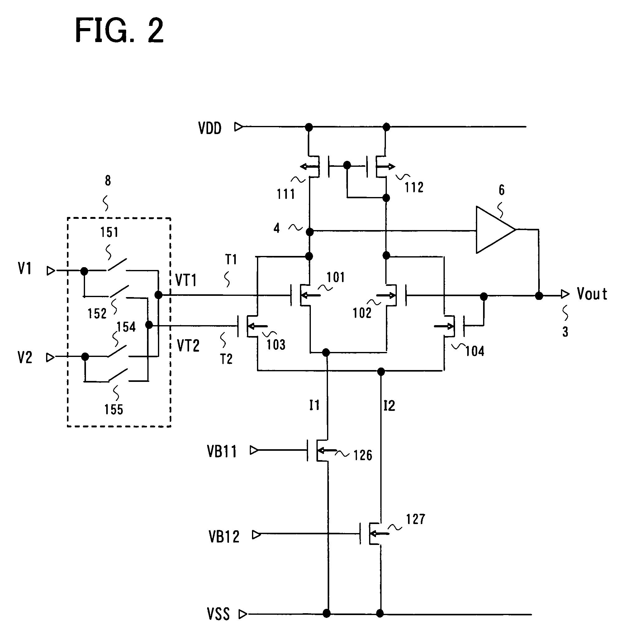
[0182]In the differential amplifier, shown in the present invention, a voltage obtained by interior division of the voltages VT1 and VT2 at the terminals T1 and T2 with a preset interior division ratio may be output. Hence, by selectively supplying the voltages V1 and V2 to the terminals T1 and T2, respectively, by the input control circuit 8, it is possible to output voltages of the same levels as the voltages V1 and V2 and voltages of two levels corresponding to interior division of the voltages V1 and V2.

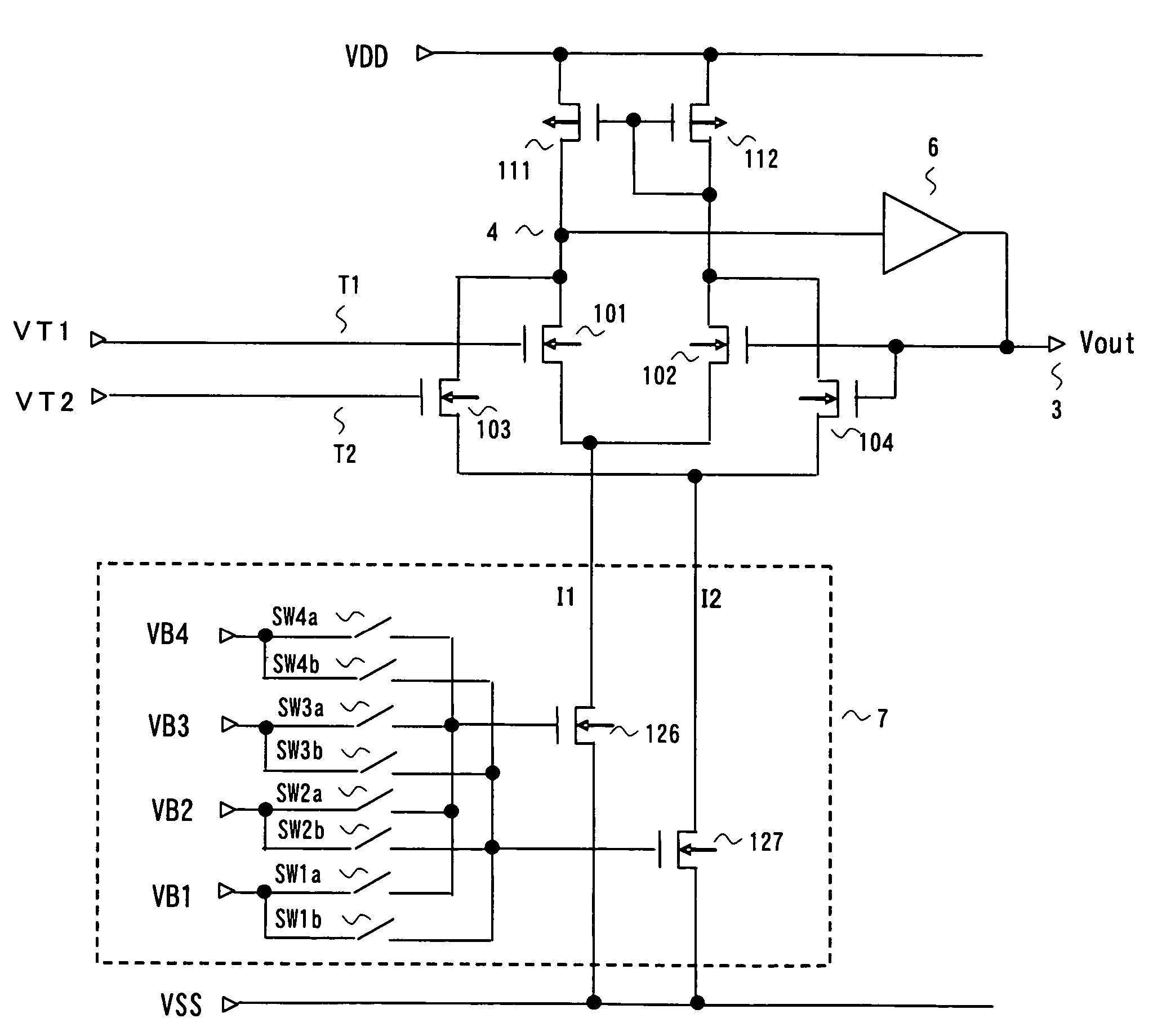
[0183]In the differential amplifiers of the first and second embodiments, shown in FIG. 1, the first differential pair (101, 102) and the second differential pair (103, 104) are n-channel transistors (same polarity type transistors). However, the differential amplifier including two differential pairs of p-channel transistors may, of course, be capable.

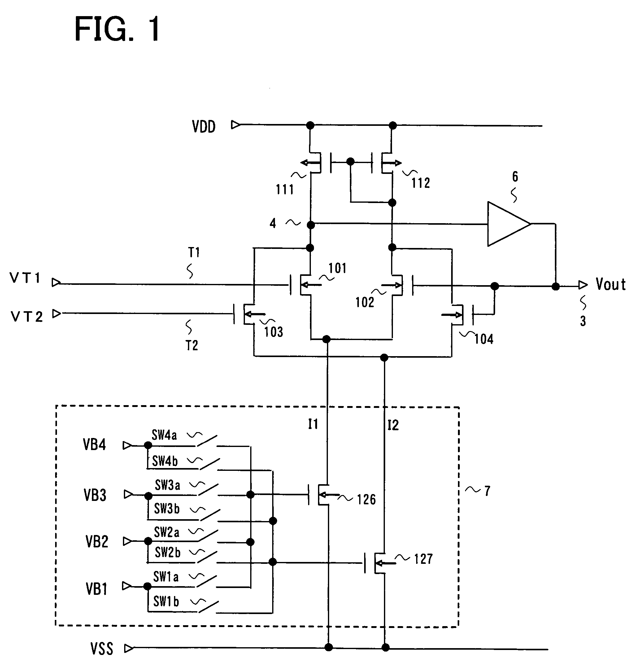
[0184]The operation of each of the first and second embodiments, shown in FIGS. 1 and 2, will now be described.

first embodiment

[0185]Initially, the operation of the above-described first embodiment of the differential amplifier, shown in FIG. 1, for a case where the respective voltages VT1 and VT2 of the terminals T1 and T2 are of different voltage values, and satisfy the condition of VT12, will be described with reference to FIGS. 3 and 4.

[0186]FIG. 3 illustrates the operation of the differential amplifier of FIG. 1 for a case where the current ratio of the currents I1 and I2 is equal to the unity.

[0187]It is assumed that the transistors of the two differential pairs (101, 102) and (103, 104) of the differential amplifier of FIG. 1 are of the same characteristics.

[0188]The current flowing through the transistors 101, 102, 103 and 104 (drain-to-source currents) are represented by Ia, Ib, Ic and Id, respectively.

[0189]FIG. 3 shows the relationship between the drain-to-source current Ids and voltage from the voltage of the power supply VSS, plotted on the ordinate and the abscissa, respectively and, more spec...

fourth embodiment

[0263]The above results are valid for a DAC of the present invention shown in FIG. 7. If, in the differential amplifier 400 shown in FIG. 7, the two differential pairs (101, 102) and (103, 104) are formed by transistors of the same characteristics and the currents I1, I2 flowing through the respective differential pairs are equal (I1=I2), the intermediate voltage of the voltages VT1 and VT2 of the terminals T1 and T2 may be output to high accuracy over a wide voltage range. Hence, the meritorious effect, described with reference to FIGS. 8 and 9, may be achieved, such that it becomes possible to reduce appreciably the number of tap voltages as compared to the number of output voltages.

[0264]FIG. 12 depicts input / output characteristics resulting from the simulation in which the two differential pairs (101, 102) and (103, 104) of the differential amplifier of FIG. 10 are constituted by transistors of the same characteristics and the current ratio of the respective currents I1 and I2 f...


PUM


Abstract

Disclosed is a differential amplifier which includes first and second input terminals, an output terminal, first and second differential pairs, and first and second current sources for supplying currents to the first and second differential pairs. The first differential pair has first and second inputs of an input pair connected to the first input terminal and the output terminal, respectively. The second differential pair has first and second inputs of an input pair connected to the second input terminal the output terminal, respectively. The differential amplifier further includes a load circuit connected to output pairs of the first and second differential pairs for outputting a signal obtained on combining outputs of the first and second differential pairs from at least one of a pair of connection nodes between the output pairs of the first and second differential pairs and the load circuit, an amplifier stage supplied with at least one signal at a connection node of the output pairs of the first and second differential pairs and the load circuit to output a voltage at the output terminal, and a current control circuit controlling the first and second current sources for controlling the ratio of currents supplied to the first and second differential pairs.

Description

FIELD OF THE INVENTION[0001]This invention relates to a differential amplifier, a display apparatus employing the differential amplifier.BACKGROUND OF THE INVENTION[0002]Recently, a liquid crystal display (LCD) apparatus, featuring thin thickness, small weight and low power usage, has come into widespread use, as display apparatus, and is used predominantly in a display section of a mobile device, such as mobile phone or cellular phone, PDA (Personal Digital Assistant) or a notebook PC. However, of these days, the technique for forming a liquid crystal display to a large size or for coping with moving pictures has been improved such that realization of a large size display apparatus of a mobile type but also of a desktop type, or a large size liquid crystal television receiver, has become feasible. For liquid crystal display apparatus, a liquid crystal display apparatus of the active matrix driving system, capable of high definition demonstration, is currently in use. Referring firs...

Claims


Application Information

Patent Timeline
Patent Type & Authority Patents(United States)
IPC IPC(8): H03F3/45
CPCH03F3/45179H03F2203/45504H03F2203/45521H03F2203/45616
Inventor TSUCHI, HIROSHI
Owner RENESAS ELECTRONICS CORP
Why Eureka
Try Eureka