Electrooptically wavelength-tunable resonant cavity optoelectronic device for high-speed data transfer

a resonant cavity and optoelectronic technology, applied in the field of semiconductor devices, can solve the problems of parasitic capacitance and inductance, high cost and precise processing tolerance, and inability to operate at very high current and dissipated power density, and achieve the effect of modulating the transmittance of the system

Inactive Publication Date: 2008-05-06
INNOLUME
View PDF29 Cites 23 Cited by
  • Summary
  • Abstract
  • Description
  • Claims
  • Application Information

AI Technical Summary

Problems solved by technology

Continuous wave (CW) operation at very high current and dissipated power densities was not possible.
Many disadvantages of laser diodes originate from parasitic radiative modes, which cause enhanced radiative leakage, thus preventing quickly approaching a population inversion.
A disadvantage of this approach is its much higher cost and precise processing tolerances, related, for example, to deep ion etching of the distributed Bragg reflector (DBR) layers.
None of the approaches for high-speed operation in the prior art address problems of parasitic capacitance, inductance and resistance in VCSELs.
In spite of the fact that low threshold quantum well and quantum dot devices exist, parasitic capacitance, inductance and resistance in VCSELs limit their high-speed performance, even when intrinsic parameters (relaxation oscillations) indicate the possibility for a much faster bit rate.
It is difficult to reduce parasitics in VCSELs and still provide certain aperture sizes, certain thicknesses of the Bragg reflector regions, certain surface areas of the current pads and unavoidable high differential capacitance of the p-n junction under direct bias.
Simultaneously approaching low threshold current, high frequency response, low power dissipation and high reliability is difficult for directly-modulated VCSELs.
However, a principal limitation is that the device must be operated at high current densities to achieve high modulation speed.
However, as the active region of the device is under a continuous population inversion condition, applying a reverse bias to change the bandgap may cause dramatic photocurrent, depleting the photopumped active region.
Mode-locked operation, however, is usually very sensitive to the conditions of the device operation and exists only in a relatively narrow range of carefully-optimized conditions.
One disadvantage of this device is the necessity of using piezoelectric materials.

Method used


Image

  • Electrooptically wavelength-tunable resonant cavity optoelectronic device for high-speed data transfer
  • Electrooptically wavelength-tunable resonant cavity optoelectronic device for high-speed data transfer
  • Electrooptically wavelength-tunable resonant cavity optoelectronic device for high-speed data transfer

Examples


Embodiment Construction

[0049]The present invention provides an ultrafast way to modulate the intensity already at the exit of an optoelectronic device.

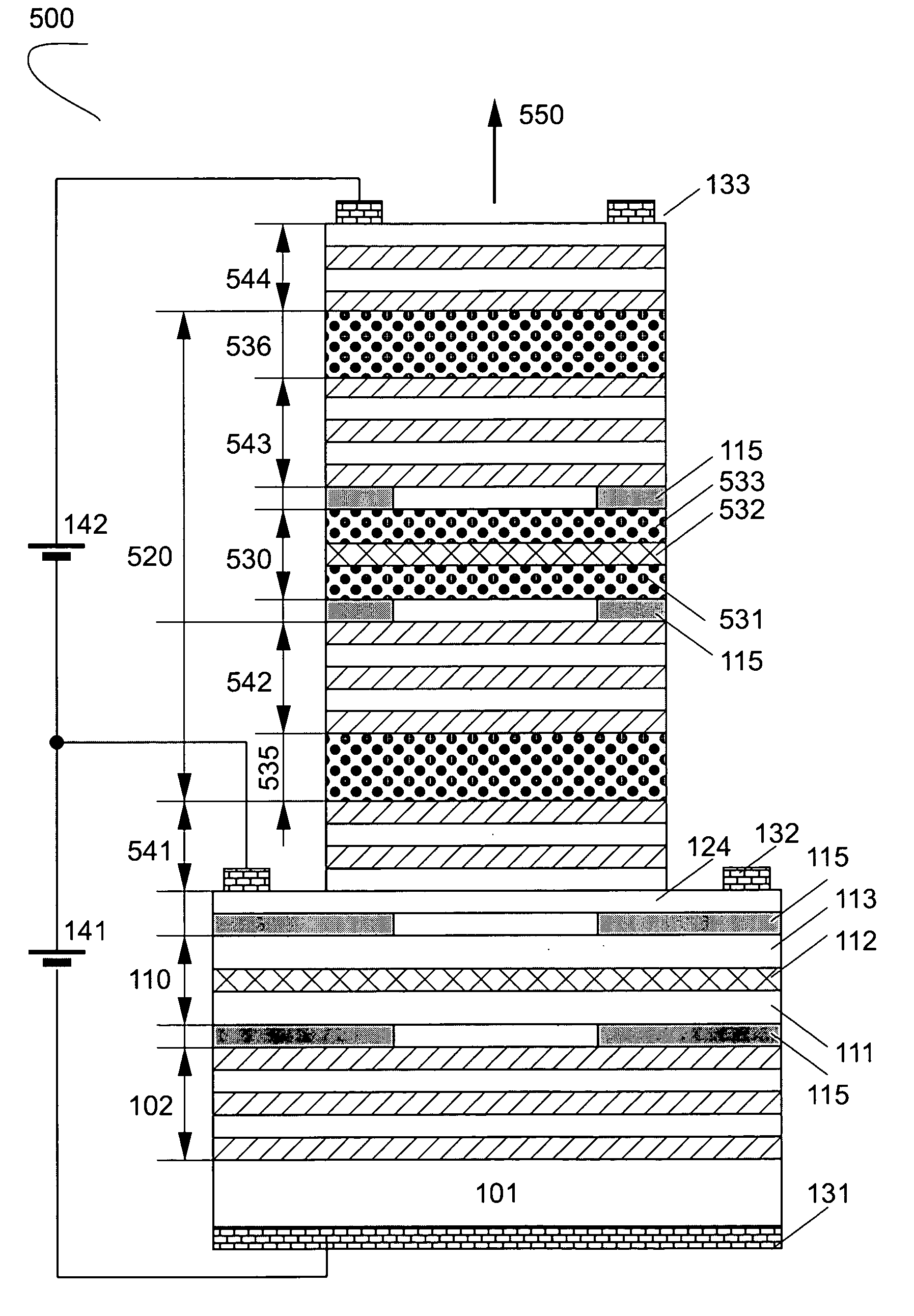
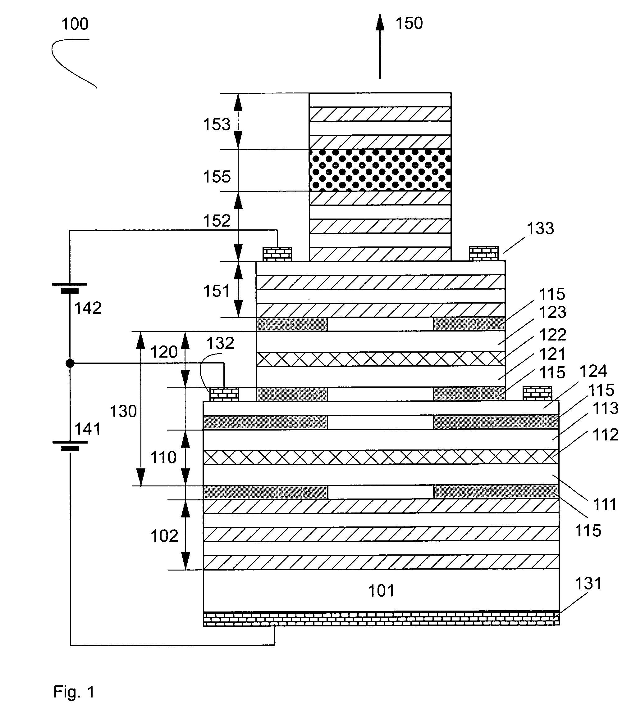
[0050]FIG. 1 shows schematically an electronically wavelength tunable vertical cavity surface emitting laser, where the modulation of the wavelength is transformed into the modulation of the intensity of the output laser light. The device 100 includes a substrate 101, a first distributed Bragg reflector 102, a cavity 130, a second distributed Bragg reflector 151, a third distributed Bragg reflector 152, a filter 155, and a fourth distributed Bragg reflector 153. The cavity 130 includes a light generating element 110, and a modulating element 120.

[0051]The part of the device 100, including the substrate 101, the first distributed Bragg reflector 102, the light generating element 110, the modulating element 120, and the second distributed Bragg reflector 151, is a wavelength tunable vertical cavity surface emitting laser as disclosed in U.S. Pat. No. 6,611,53...


PUM


Abstract

A device contains at least one wavelength-tunable element controlled by an applied voltage and at least two resonant cavities, where the resonant wavelength of the tunable element is preferably elecrooptically tuned using the quantum confined Stark effect around the resonant wavelength of the other cavity or cavities, resulting in a modulated transmittance of the system. A light-emitting medium is preferably introduced into one of the cavities, permitting the optoelectronic device to work as an intensity-modulated light-emitting diode or diode laser by applying an injection current. The device preferably contains at least three electric contacts to apply a forward or a reverse bias and may operate as a vertical cavity surface emitting light-emitter or modulator or as a tilted cavity light emitter or modulator. Adding a few modulator sections enables applications in semiconductor optical amplifiers, frequency converters or lock-in optical amplifiers.

Description

REFERENCE TO RELATED APPLICATIONS[0001]This application claims an invention which was disclosed in Provisional Application No. 60 / 577,537, filed Jun. 7, 2004, entitled “ELECTROOPTICALLY WAVELENGTH-TUNABLE RESONANT CAVITY OPTOELECTRONIC DEVICE FOR HIGH-SPEED DATA TRANSFER”. The benefit under 35 USC §119(e) of the United States provisional application is hereby claimed, and the aforementioned application is hereby incorporated herein by reference.BACKGROUND OF THE INVENTION[0002]1. Field of the Invention[0003]The invention pertains to the field of semiconductor devices. More particularly, the invention pertains to ultrahigh-speed optoelectronic devices.[0004]2. Description of Related Art[0005]High-speed optoelectronic devices are broadly applied in modem datacommunication and telecommunication systems.[0006]These devices can be separated into two categories: those directly modulated by injection of current into the gain region, and those externally modulated. Direct-modulation offers ...

Claims


Application Information

Patent Timeline
Patent Type & Authority Patents(United States)
IPC IPC(8): H01S3/10G02B5/28H01S3/08H01S5/026H01S5/06H01S5/10H01S5/183H01S5/343
CPCH01S5/0607H01S5/1021H01S5/18302G02B5/28H01S5/0078H01S5/18311H01S5/1833H01S5/18341H01S5/2027
Inventor LEDENTSOV, NIKOLAISHCHUKIN, VITALY
Owner INNOLUME
Why Eureka
Try Eureka