
Method and apparatus for controlling slope of word line voltage in nonvolatile memory device

a nonvolatile, memory device technology, applied in static storage, digital storage, instruments, etc., can solve the problems of parasitic coupling capacitance, high integration, and the ability of nand flash memory devices to only perform erase operations in the unit of one memory block

Active Publication Date: 2008-05-13
SAMSUNG ELECTRONICS CO LTD
View PDF7 Cites 22 Cited by
  • Summary
  • Abstract
  • Description
  • Claims
  • Application Information

AI Technical Summary

Benefits of technology

The patent text describes a method and apparatus for controlling the slope of a word line voltage in a nonvolatile semiconductor memory device. The invention relates to a flash memory device, which is a type of nonvolatile semiconductor memory that can store data even when power is turned off. The invention provides a method for controlling the threshold voltage of a flash memory cell, which is the minimum voltage required to turn on the cell, by adjusting the slope of the word line voltage. The invention also includes a method for erasing and programming the flash memory cells. The technical effect of the invention is to improve the speed and reliability of the flash memory device by controlling the threshold voltage of the memory cells and optimizing the erase and programming operations.

Problems solved by technology

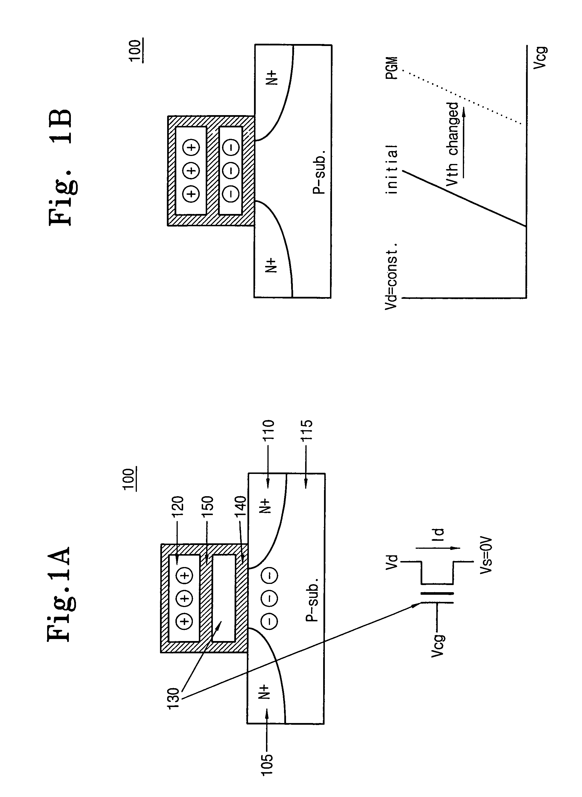
In the volatile semiconductor memories, data are stored and can be read out as long as the power is applied, and are lost when the power is turned off.
The NOR-type flash memory can be easily adapted to high-speed operation, but has a disadvantage when it comes to providing a high degree of integration.
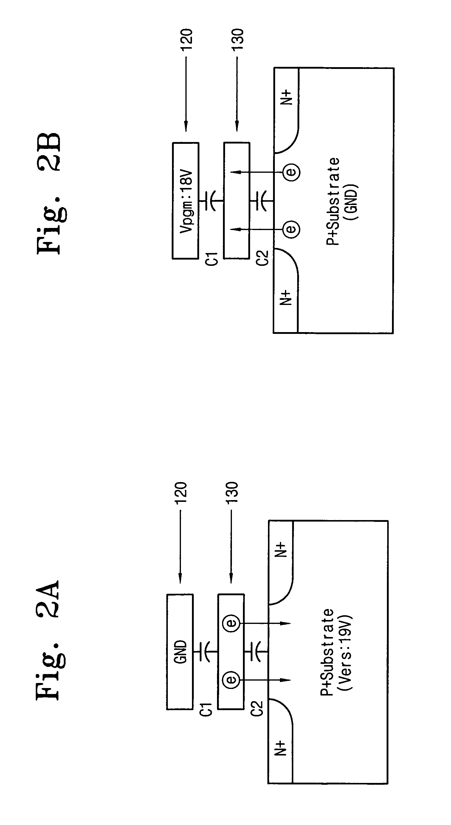
However, the NAND flash memory device can only perform an erase operation in the unit of one memory block.
However, there is a problem with the flash memory cell programming techniques described above, including the ISSP technique.
As illustrated in FIG. 11, this parasitic coupling capacitance can create a problem when word line 31 is selected during a flash memory cell program operation.
VPASS has a voltage level such that when the bit line is grounded, the voltage is sufficient to turn on the memory cells connected with these unselected word lines, but insufficient to program these memory cells.
In other words, the program inhibit operation may fail.
Moreover, due to the coupling capacitances, a similar problem may also occur when another word line (e.g., word line 30) located near the SSL is selected.

Method used


Image

  • Method and apparatus for controlling slope of word line voltage in nonvolatile memory device
  • Method and apparatus for controlling slope of word line voltage in nonvolatile memory device
  • Method and apparatus for controlling slope of word line voltage in nonvolatile memory device

Examples


first embodiment

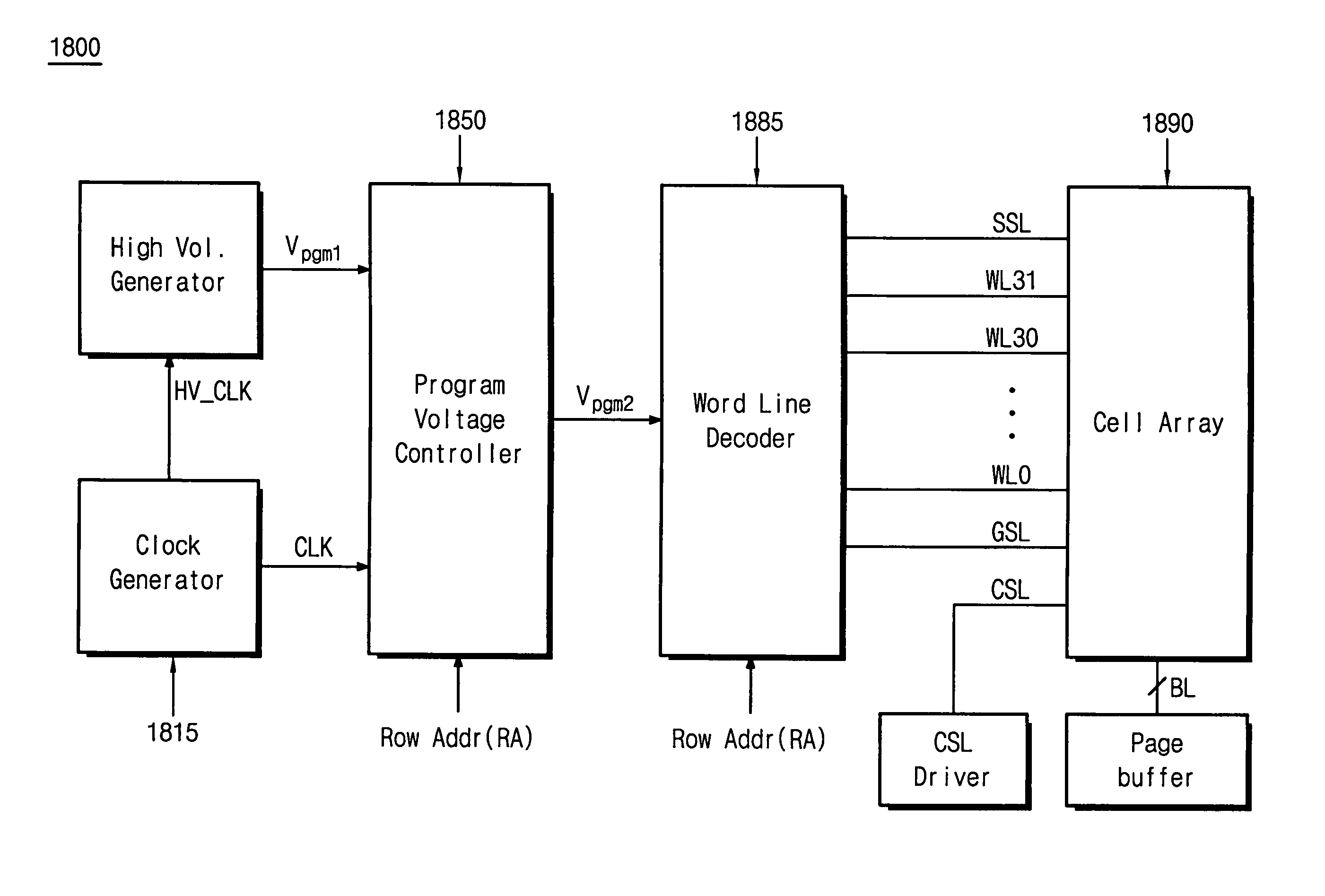
[0068]FIG. 19 shows a detailed block diagram of a word line voltage generator 1900. Word line voltage generator 1900 includes a voltage ladder 1920, a step voltage controller 1940, and a time controller 1960. Voltage ladder 1920 receives a sequence of voltage pulses VPGM1, and produces therefrom a plurality of voltages, V0, V1, V2, . . . , Vn-1. Time controller 1960 outputs a clock signal having a plurality of substantially equal time periods. Step voltage controller 1940 receives the clock signal from time controller 1960 and selects a voltage from voltage ladder 1920 in each of a plurality of time periods to control the slope of at least one of the voltage pulses in response to a ROW address corresponding to the selected word line. That is, step voltage controller 1940 sets a magnitude of the voltage in each clock period according to the ROW address of the selected word line, and thereby controls a slope (rise time) of the voltage pulse according to the position of the selected wo...

second embodiment

[0070]FIG. 21 shows a detailed block diagram of a word line voltage generator 2100. Word line voltage generator 2100 includes a voltage ladder 2120, a step voltage controller 2140, and a time controller 2160. Voltage ladder 2120 receives a sequence of voltage pulses VPGM1, and produces therefrom a plurality of voltages, V0, V1, V2, . . . , Vn-1. Time controller 2160 outputs a clock signal having a plurality of time periods. Step voltage controller 2140 receives the clock signal from time controller 2160 and in response thereto increments the voltage from voltage ladder 2120 by a predetermined amount in each of the plurality of time periods. Beneficially, time controller 2160 sets the time periods to control the slope of at least one of the voltage pulses in response to a row address corresponding to the selected word line. That is, time controller 2160 sets a time period of each clock period according to the ROW address of the selected word line, and thereby controls a slope (rise t...

third embodiment

[0073]FIG. 23 shows a detailed block diagram of a word line voltage generator 2300. Word line voltage generator 2300 includes a pulse voltage generator (not shown), a word line slope controller 2320, a multiplexer 2340, and a word line detector 2360. The pulse voltage generator generates a first sequence of voltage pulses VPGM1 to be applied to a selected word line for programming memory cells of a nonvolatile memory cell array (also not shown). Beneficially, the pulse voltage generator outputs the first sequence of voltage pulses according to the incremental step pulse program (ISPP) technique. Word line slope controller 2320 receives the first sequence of voltage pulses VPGM1 and controls the slope of at least one of the voltage pulses VPGM1 of the first sequence to thereby generate a second sequence of voltage pulses VPGM2. Beneficially, the first and second sequences of voltage pulses VPGM1 and VPGM2 may be any of the pairs of sequences shown in any of FIGS. 14-16 above. Multipl...


PUM


Abstract

A nonvolatile memory device includes a nonvolatile memory cell array including a plurality of nonvolatile memory cells connected to a plurality of word lines, a word line voltage generator configured to generate first and second sequences of voltage pulses. The device selectively supplies one of the first and second sequences of voltage pulses to a selected one of the word lines to program the nonvolatile memory cells connected to the selected word line. A slope of at least one voltage pulse of the first sequence of voltage pulses is greater than a slope of at least one voltage pulse of the second sequence of voltage pulses. In general, the first sequence is applied to word lines far away from the string select line (SSL), and the second sequence is applied to word lines that are close to the SSL.

Description

BACKGROUND AND SUMMARY[0001]1. Field[0002]This invention relates, in general, to nonvolatile semiconductor memory devices and, more particularly, to a method and apparatus for controlling the slope of a word line voltage in a nonvolatile semiconductor memory device, a nonvolatile semiconductor memory device including such an apparatus and executing such a method, and a memory system including such a nonvolatile semiconductor memory device.[0003]2. Description[0004]Semiconductor memories are classified into volatile semiconductor memories and non-volatile semiconductor memories. In the volatile semiconductor memories, data are stored and can be read out as long as the power is applied, and are lost when the power is turned off. On the other hand, non-volatile memories such as an MROM (MASK ROM), a PROM (Programmable ROM), an EPROM (Erasable and Programmable ROM), an EEPROM (Electrically Erasable and Programmable ROM), and flash memories are capable of storing data even with the power...

Claims


Application Information

Patent Timeline
Patent Type & Authority Patents(United States)
IPC IPC(8): G11C7/00
CPCG11C16/0483G11C16/10G11C16/12G11C16/30G11C16/32
Inventor HWANG, SANG-WONLEE
Owner SAMSUNG ELECTRONICS CO LTD
Learn More