Stamper and transfer apparatus

a transfer apparatus and stamper technology, applied in the field of stampers, can solve the problems of inability to accurately transfer fine structures on the order of micrometers, and the pattern on the stamper surface cannot be correctly transferred to the resin, etc., to achieve accurate transfer, high modulus of elasticity, and accurate transfer

Inactive Publication Date: 2008-05-20
HITACHI LTD
View PDF18 Cites 21 Cited by
  • Summary
  • Abstract
  • Description
  • Claims
  • Application Information

AI Technical Summary

Benefits of technology

[0010]A pattern formed on the surface of a stamper can be accurately transferred without being affected by any distribution of convex portions of the surface of the stamper or any contour of a substrate, by forming, on a back side of the stamper, a buffer with a distribution of moduli of elasticity.
[0011]In one aspect, the invention provides a method of using a stamper that is backed with a buffer having a distribution of moduli of elasticity such that a portion of the buffer that corresponds to a portion of the stamper that has more convex portions has a high modulus of elasticity, as shown in FIG. 1. The buffer having such a distribution of moduli of elasticity can apply a force to the stamper that is commensurate with the distribution of resistance the stamper experiences from an organic resin layer due to the distribution of convex portions of the ...

Problems solved by technology

These height irregularities pose an obstacle in accurately transferring fine structures on the order of micrometers or less.
As a result, these areas receive a larger ...

Method used


Image

  • Stamper and transfer apparatus
  • Stamper and transfer apparatus
  • Stamper and transfer apparatus

Examples


example 1

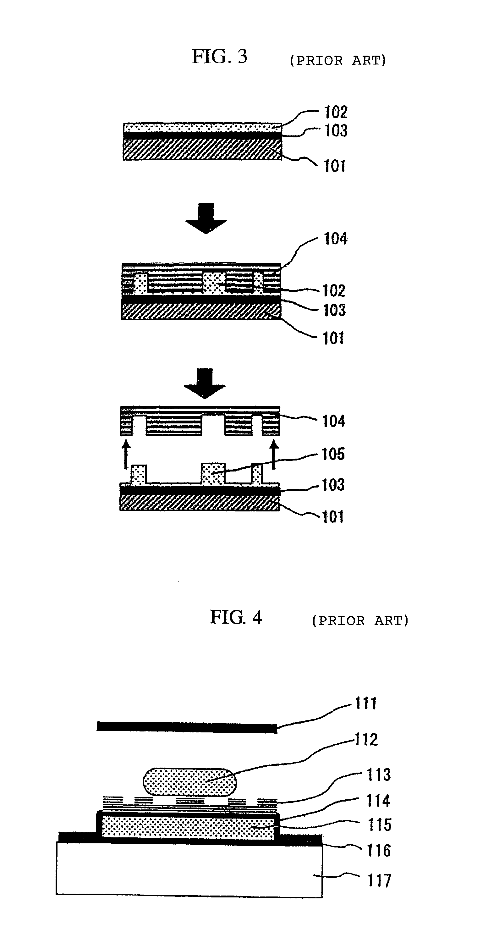
[0029]An embodiment of the invention will be hereafter described. FIG. 5 shows an example of a transfer process in one aspect of the invention.

[0030]First, an organic resin layer 202 of PMMA (poly(methyl-methacrylate)) was formed on a silicon wafer substrate 201 with a crystal orientation (100) and a diameter of 150 mm, using a spin coat method. The organic resin layer 202 had a thickness of 1 μm and a melting point of approximately 220° C.

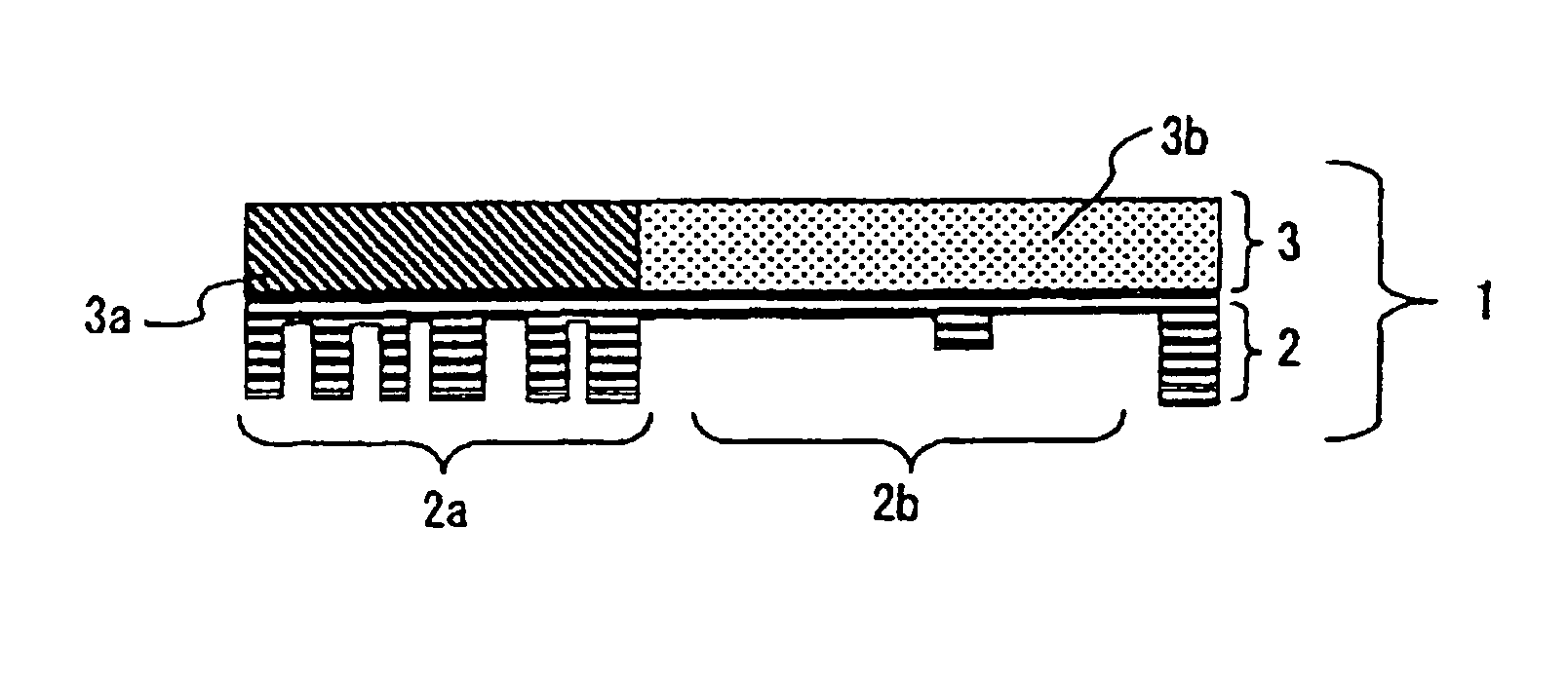
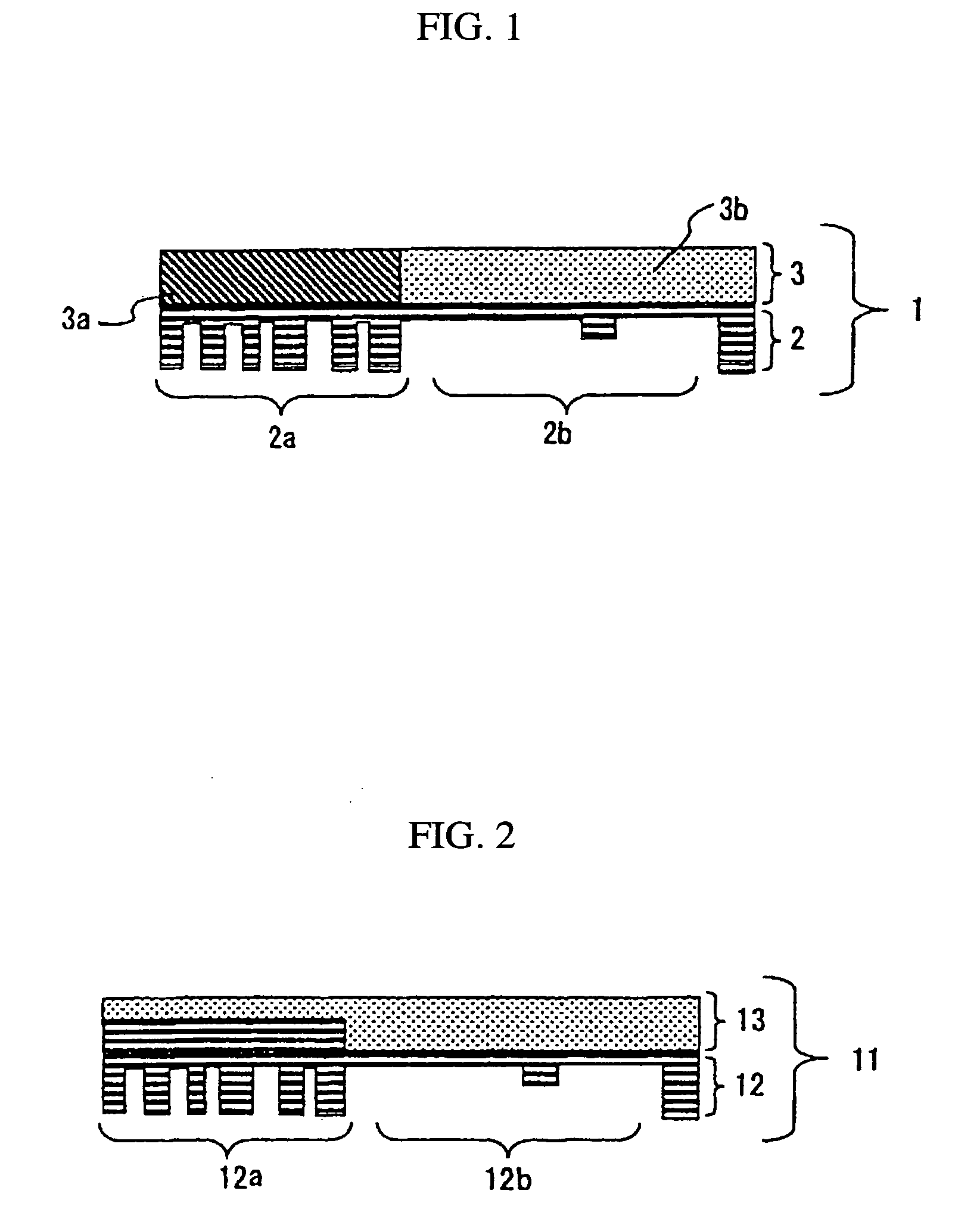
[0031]FIG. 1 shows a stamper 1 used in the present embodiment. The stamper 1 comprised a flexible stamper layer 2 of a nickel-electroformed film and a buffer 3. The buffer 3 was patterned by a screen printing method such that the modulus of elasticity had a longitudinal distribution. Specifically, the buffer 3 is patterned with portions with a high and a low modulus of elasticity in accordance with the density of convex portions of the flexible stamper layer 2, such that a portion 3a with a high modulus of elasticity corresponds to a portion 2a of...

example 2

[0038]Another example of the invention will be described. FIG. 6 shows an example of a transfer process according to another aspect of the invention.

[0039]An organic resin layer 202 of PMMA with a crystal orientation (100) was formed on a silicon wafer substrate 201 with a diameter of 150 mm by a spin coat method. The organic resin layer 202 had a thickness of 1 μm and a melting point of about 220° C.

[0040]FIG. 2 shows a stamper 11 used in the present example. The stamper 11 comprised a flexible stamper layer 12 made of a nickel-electroformed film, and a buffer 13. The buffer 13 was patterned with various thicknesses in accordance with the density of the convex portions of the surface of the flexible stamper layer 2. Specifically, a portion of the stamper that corresponds to a portion 12a of the surface of the flexible stamper layer 12 that had more convex portions was formed to be thin, while a portion of the stamper that corresponds to a portion 12b of the surface of the flexible ...

example 3

Biochip

[0048]FIG. 8 schematically shows a biochip 900. In a substrate 901 made of glass is formed a passage 902 with a depth of 3 μm and a width of 20 μm. A specimen containing DNA (deoxyribonucleic acid), blood, protein, or the like is introduced via an inlet 903 and is caused to flow in the passage 902 until it reaches an outlet 904. A molecular filter 905 is disposed in the passage 902. In the molecular filter 905, there is formed a projection assembly 100 measuring 250 to 300 nm in diameter and 3μm in height. FIG. 7 shows an enlarged view of the projection assembly 100.

[0049]FIG. 9 is a perspective view of the biochip 900 near where the molecular filter 905 is formed. The projection assembly 100 is formed in a part of the passage 902 formed on the substrate 901. The substrate 901 is covered with an upper substrate 913 so that the specimen flows inside the passage 902. In the case of a DNA chain-length analysis, while a specimen containing DNA is electrophoresed in the passage 90...


PUM

PropertyMeasurementUnit
Thicknessaaaaaaaaaa
Structureaaaaaaaaaa
Flexibilityaaaaaaaaaa

Abstract

A stamper and a transfer apparatus that utilizes the stamper, which is capable of accurately transferring its own pattern onto an article, such as a substrate, without being affected by any distribution of convex portions on the stamper surface or any contour of the substrate. The stamper has a fine concave-convex pattern on a surface thereof for forming a fine structure on a substrate using a pressing machine. The stamper is flexible and includes a buffer formed on an opposite side to the side on which the concave-convex pattern is formed. The buffer has a longitudinal distribution of moduli of elasticity.

Description

BACKGROUND OF THE INVENTION[0001]1. Technical Field[0002]The present invention relates to a stamper for forming a fine pattern or a structure on a substrate. It also relates to a transfer apparatus using the stamper.[0003]2. Background Art[0004]FIG. 3 schematically illustrates the process of forming a mask pattern on a thin film provided on a substrate by applying an organic resin to the substrate and then molding the organic resin with a stamper. A stamper 104 is moved over a substrate 101 on which a thin film 103 and an organic resin layer 102 have been formed, while pressing evenly the stamper onto the organic resin layer 102 that has not been cured, thereby transferring a pattern formed on the stamper onto the organic resin layer 102. After the transfer of the pattern, the organic resin layer 102 is heated or irradiated with light so as to cure the organic resin layer 102 and thus fix its shape, thereby forming a mask pattern 105 to be used as a protective mask for etching. Usin...

Claims


Application Information

Patent Timeline
IPC IPC(8): B29C43/10B32B3/00G11B7/26B29C33/38B29C43/18B29L17/00G03F7/00G11B5/84
CPCB82Y10/00B82Y40/00G03F7/0002G03F7/0017Y10S425/81
Inventor KUWABARA, KOSUKEMIYAUCHI, AKIHIROOGINO, MASAHIKOMOTOWAKI, SIGEHISA
Owner HITACHI LTD
Why Eureka
Try Eureka