Method of manufacturing microlens, microlens, optical film, screen for projection, projector system, electrooptical device and electronic equipment

a manufacturing method and technology for microlens, applied in the field of manufacturing microlens, microlens, optical films, screens for projection, electrooptical devices and electronic equipment, can solve the problems of insufficient overall manufacturing process, inability to fully utilize the advantages of droplet discharge methods, and difficulty in heaping droplets beyond contact angles, etc., to achieve the effect of fine optical characteristics, simple manufacturing and efficient manufacturing

Inactive Publication Date: 2008-05-20
SEIKO EPSON CORP
View PDF11 Cites 15 Cited by
  • Summary
  • Abstract
  • Description
  • Claims
  • Application Information

AI Technical Summary

Benefits of technology

[0010]An advantage of the invention is to provide a simple manufacturing method of a microlens, a microlens and a optical film with fine optical characteristics, a screen for projection, a projector system, an electrooptical device and electronic equipment.
[0011]According to a first aspect of the invention, a method of manufacturing a microlens having a convex shape on a substrate including a step of providing a first droplet on the substrate, a step of forming a first convex portion by drying the first droplet so as to solidify the first droplet, a step of providing a second droplet of a lens material in a concave area that is placed at a center of the first convex portion and a step of forming a second convex portion by curing the second droplet.
[0012]According to the first aspect of the invention, the first convex portion having the concave area at its center is formed because of the so called coffee stain phenomenon when the first droplet is dried so as to be solidified. The microlens can be formed only by the droplet discharge method, if the second droplet of the lens material is provided in the concave area of the convex portion and then dried so as to be cured. Therefore, the manufacturing process becomes efficient because there is no need of an exposure step and a developing step. Furthermore, by utilizing the contact angle of the convex portion, it is possible to increase the amount of the droplet heaping up in the convex portion and to form the microlens with a larger curvature or a high aspect ratio.
[0013]In this case, it is preferable that the substrate is made liquid-repellent before the first droplet is provided. This means that the size of the first droplet disposed on the substrate tends to become smaller because the first droplet of the bank material is repelled on the substrate. Accordingly, the first convex portion can be formed smaller and denser. Furthermore, the microlens with the high curvature or aspect ratio can also be formed by disposing the lens material in the form of the second droplet on the first convex portion because the first convex portion is made liquid repellent.
[0014]It is also preferable that the first convex portion is made liquid-repellent before the second droplet is provided.
[0015]Since the first convex portion is made liquid-repellent, it is possible to increase the curvature or aspect ratio of the microlens if the lens material in the form of the second droplet is provided on the first convex portion.

Problems solved by technology

However, it is difficult to heap up the droplet beyond the contact angle.
Accordingly, the overall manufacturing process becomes insufficient.
In other words, the hitherto known manufacturing methods did not fully utilize the advantages of the droplet discharge method.

Method used


Image

  • Method of manufacturing microlens, microlens, optical film, screen for projection, projector system, electrooptical device and electronic equipment
  • Method of manufacturing microlens, microlens, optical film, screen for projection, projector system, electrooptical device and electronic equipment
  • Method of manufacturing microlens, microlens, optical film, screen for projection, projector system, electrooptical device and electronic equipment

Examples


first modification example

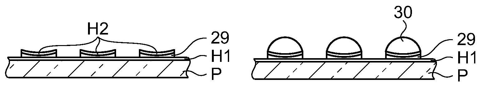
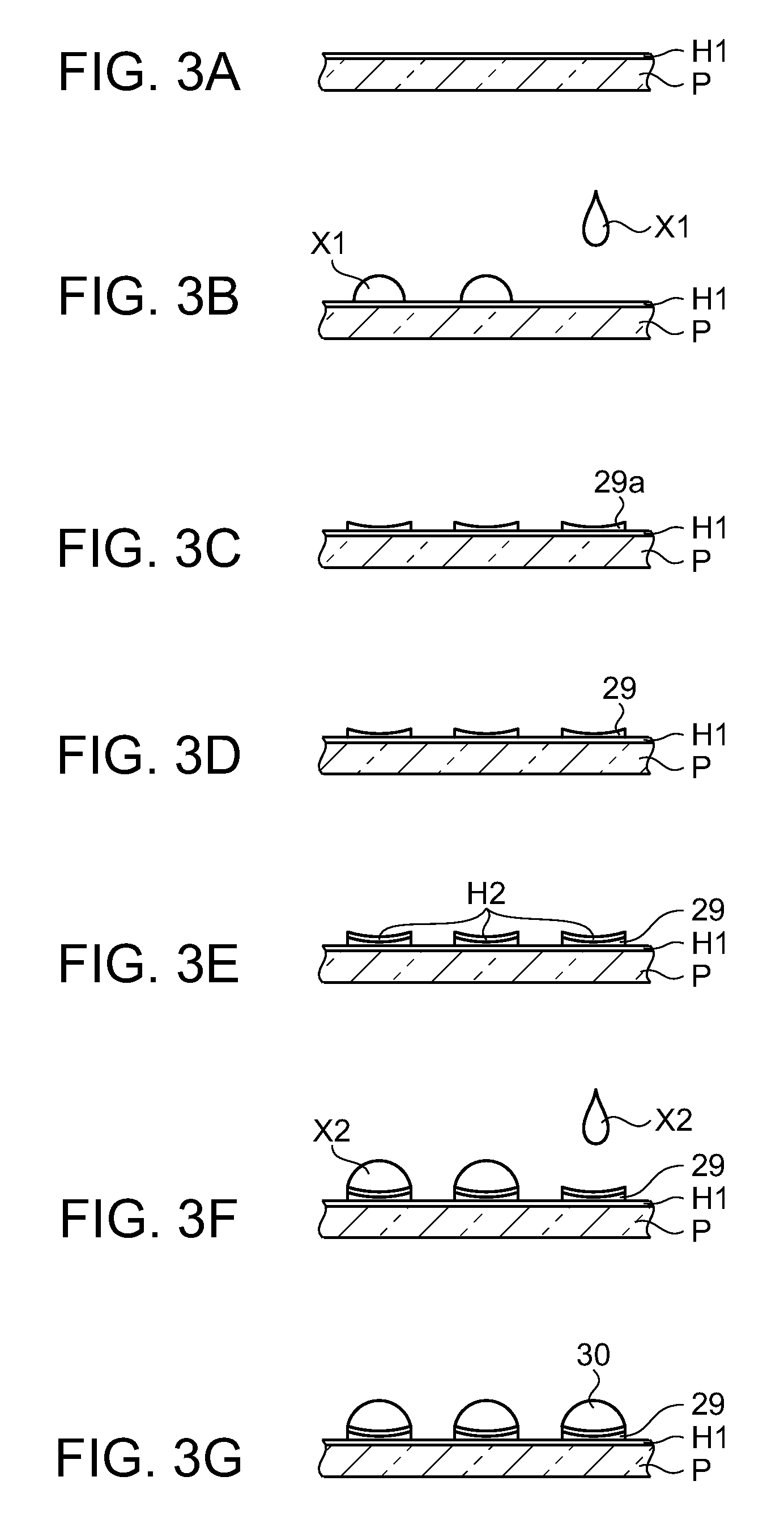
[0180]Though the bank 29 which is the first convex portion is made of the different material from that of the microlens in the above described embodiment, the material is not limited to this. For example, the bank 29 may be formed of the same material as that of the microlens. In this case, the manufacturing process becomes simpler and it has the same refractive index as that of the microlens.

second modification example

[0181]Though the surface of the substrate P is made liquid repellent and the liquid-repellant layer H1 is formed onto in the above described embodiment, the surface treatment is not limited to the liquid repellent treatment. For example, the surface of the substrate P may be made liquid-attracting. In this case, it is possible to make the diameter of the bank 29 larger. Accordingly, the diameter of the microlens becomes larger.

third modification example

[0182]Though the microlens 30 is used in the screen for projection and in the projector system in the above described embodiment, the use of the microlens is not limited to this. For example, the microlens can be used as an optical component of a head for a leaser printer, a light acceptance face of a solid-state image pickup device (charge-coupled device), an optical coupling part of an optic fiber system, a light transmission device and the like.


PUM

PropertyMeasurementUnit
carbon numberaaaaaaaaaa
temperatureaaaaaaaaaa

Abstract

A method of manufacturing a microlens having a convex shape on a substrate includes: a step of providing a first droplet on the substrate, a step of forming a first convex portion by drying the first droplet so as to solidify the first droplet, a step of providing a second droplet of a lens material in a concave area that is placed at a center of the first convex portion and a step of forming a second convex portion by curing the second droplet.

Description

BACKGROUND OF THE INVENTION[0001]1. Technical Field[0002]The present invention relates to a method of manufacturing a microlens, a microlens, an optical film, a screen for projection, a projector system, an electrooptical device and electronic equipment.[0003]2. Related Art[0004]Various display devices (electrooptical devices) are equipped with color filters in order to display in color. The color filter consists of a substrate made of, for example, glass and substrate, and filter elements colored with various colors such as red (R), green (G) and blue (B) and fabricated on the substrate in the form of dots. The filter elements are arranged in a certain pattern such as so-called stripe, delta and mosaic arrangement on the substrate.[0005]The electrooptical device including a liquid crystal device and an electroluminescence (EL) device as a display has display dots arranged on a substrate of such as glass and plastic. An optical state in each display dot is independently controllable...

Claims


Application Information

Patent Timeline
Patent Type & Authority Patents(United States)
IPC IPC(8): G02B27/10B05D1/26B29D11/00G02B3/00G02F1/13357G03B21/10G03B21/62
CPCB29D11/00365B29D11/0073G02B3/0012G02B3/0018G02B3/0056G02B3/0062G02B5/201
Inventor TOYODA, NAOYUKI
Owner SEIKO EPSON CORP
Why Eureka
Try Eureka