Sub-lithographic gate length transistor using self-assembling polymers

a transistor and sub-lithographic technology, applied in the field of self-assembling copolymer forming of sub-lithographic gate length transistors, can solve the problems of increasing roughness and achieve the effects of reducing process window and product performance degradation, avoiding defects such as line edge roughness and cd variation

Active Publication Date: 2008-06-10
ELPIS TECH INC
View PDF7 Cites 19 Cited by
  • Summary
  • Abstract
  • Description
  • Claims
  • Application Information

AI Technical Summary

Benefits of technology

[0008]Line edge roughness (LER) from conventional lithography illumination and photoresist processing leads to device parameter fluctuation and device mismatch, resulting in reduced process window and product performance degradation. As device dimension scales, the impact of roughness increases. LER can be measured statistically using a variability parameter called variance or ‘sigma’. The 3-sigma of conventional patterned gate stacks is greater than 6 nm.
[0010]In another aspect of the present invention, a method of fabricating a semiconductor structure including at least one transistor having a sub-lithographic channel length located on a surface of a semiconductor substrate is provided. The method of the present invention combines conventional lithographic technology and a copolymer self-assembling technique to place one polymer unit with precise position. The polymer is self-aligned to the pre-defined lithographically defined pattern boundaries. The single polymer can then be selectively removed and the remaining polymer is used as a photo mask to pattern a transistor gate. The final feature size is determined by the polymer molecule rather than conventional lithography. Because conventional lithography is not used in providing the final gate transistor, defects such as line edge roughness and CD variation are avoided.

Problems solved by technology

Line edge roughness (LER) from conventional lithography illumination and photoresist processing leads to device parameter fluctuation and device mismatch, resulting in reduced process window and product performance degradation.
As device dimension scales, the impact of roughness increases.

Method used


Image

  • Sub-lithographic gate length transistor using self-assembling polymers
  • Sub-lithographic gate length transistor using self-assembling polymers
  • Sub-lithographic gate length transistor using self-assembling polymers

Examples


Embodiment Construction

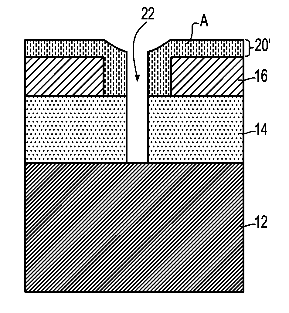
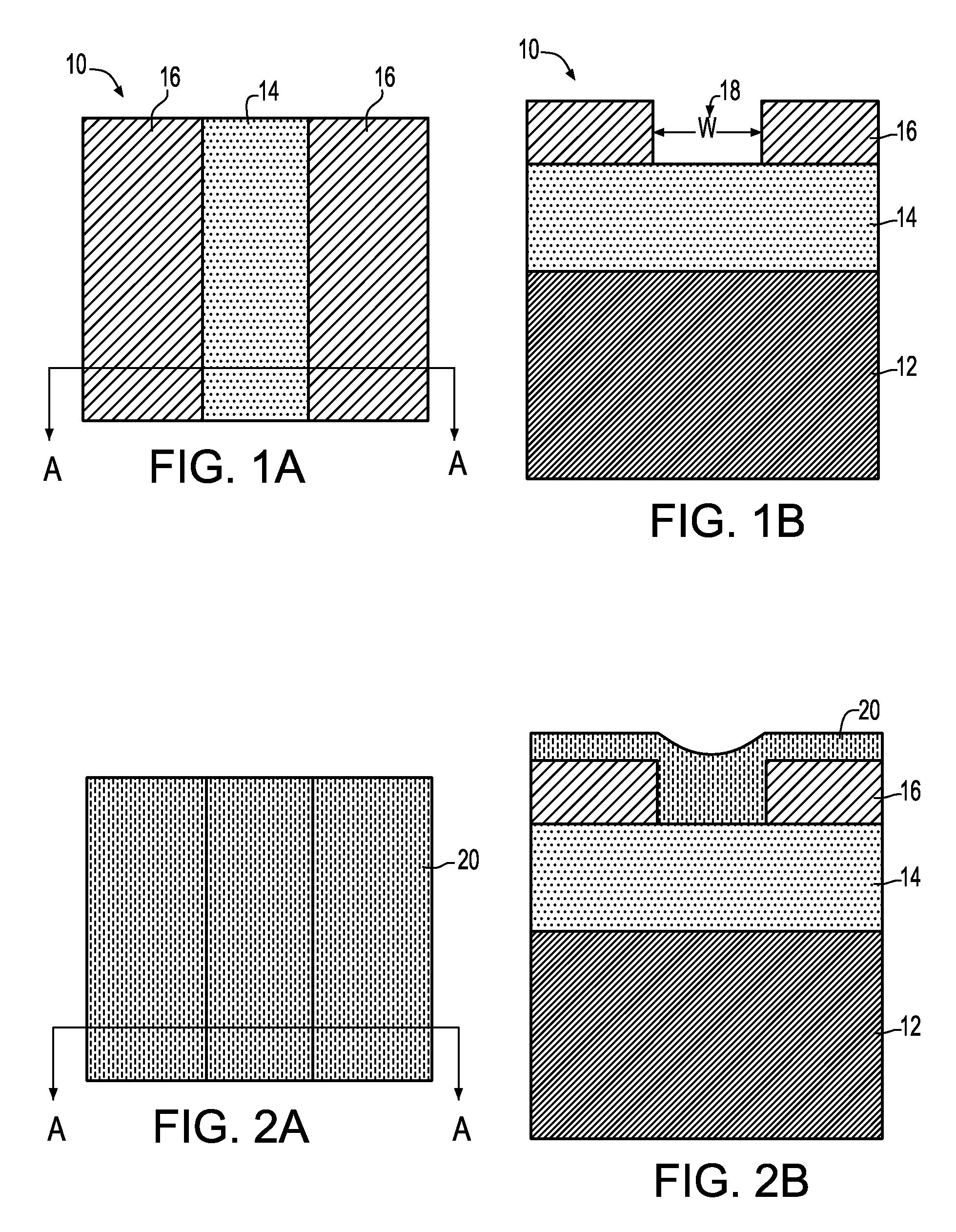
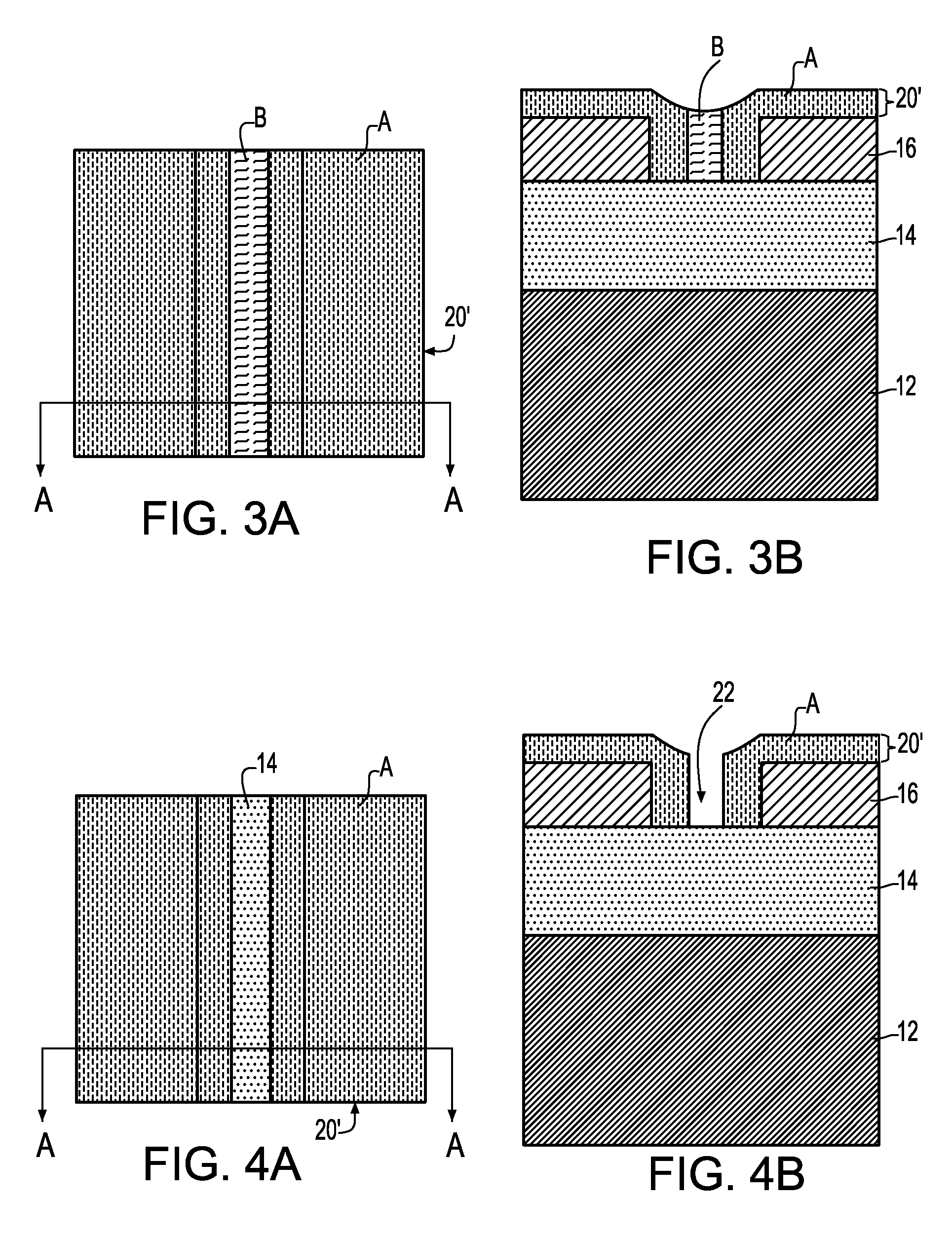
[0031]The present invention, which provides a semiconductor structure including at least one transistor having a sub lithographic gate length and a method of fabricating the same, will now be described in greater detail by referring to the following description and drawings that accompany the present application. It is noted that the drawings of the present invention are provided for illustrative purposes and, as such, they are not drawn to scale. In each of the drawings, drawing A is a top-down view and drawing B is a cross sectional view through line A-A.

[0032]In the following description, numerous specific details are set forth, such as particular structures, components, materials, dimensions, processing steps and techniques, in order to provide a thorough understanding of the present invention. However, it will be appreciated by one of ordinary skill in the art that the invention may be practiced without these specific details. In other instances, well-known structures or proces...


PUM


Abstract

A semiconductor structure including at least one transistor located on a surface of a semiconductor substrate, wherein the at least one transistor has a sub-lithographic channel length, is provided. Also provided is a method to form such a semiconductor structure using self-assembling block copolymer that can be placed at a specific location using a pre-fabricated hard mask pattern.

Description

FIELD OF THE INVENTION[0001]The present invention relates to semiconductor device manufacturing, and more particularly to a method of forming a transistor having a sub-lithographic gate length using self-assembling copolymers. The present invention also relates to a semiconductor structure including at least one transistor having a sub-lithographic gate length.BACKGROUND OF THE INVENTION[0002]Over the past twenty-five years or so, the primary challenge of very large scale integration (VLSI) has been the integration of an ever-increasing number of metal oxide semiconductor field effect transistor (MOSFET) devices with high yield and reliability. This was achieved mainly in the prior art by scaling down the MOSFET channel length without excessive short-channel effects. As is known to those skilled in the art, short-channel effects are the decrease in threshold voltage Vt in short-channel devices due to two-dimensional electrostatic charge sharing between the gate and the source / drain ...

Claims


Application Information

Patent Timeline
Patent Type & Authority Patents(United States)
IPC IPC(8): H01L21/336H01L21/8242H01L21/8228
CPCB81C1/00031B82Y30/00H01L21/0337H01L21/0338H01L21/28123H01L21/31144H01L29/66583B81C2201/0149H01L29/78G03F7/0002
Inventor YANG, HAININGLI, WAI-KIN
Owner ELPIS TECH INC
Why Eureka
Try Eureka