Metal contact structure for solar cell and method of manufacture

a technology of contact structure and solar cell, applied in the field of solar cells, can solve the problem of limiting the efficiency of photovoltaic cells in directly converting solar energy to electricity to less than 30%

Active Publication Date: 2008-06-17
CREDIT SUISSE CAYMAN ISLANDS BRANCH +1
View PDF14 Cites 164 Cited by
  • Summary
  • Abstract
  • Description
  • Claims
  • Application Information

AI Technical Summary

Problems solved by technology

These and other losses limit the efficiency of photovoltaic cells in directly converting solar energy to electricity to less than 30%.

Method used


Image

  • Metal contact structure for solar cell and method of manufacture
  • Metal contact structure for solar cell and method of manufacture
  • Metal contact structure for solar cell and method of manufacture

Examples


Embodiment Construction

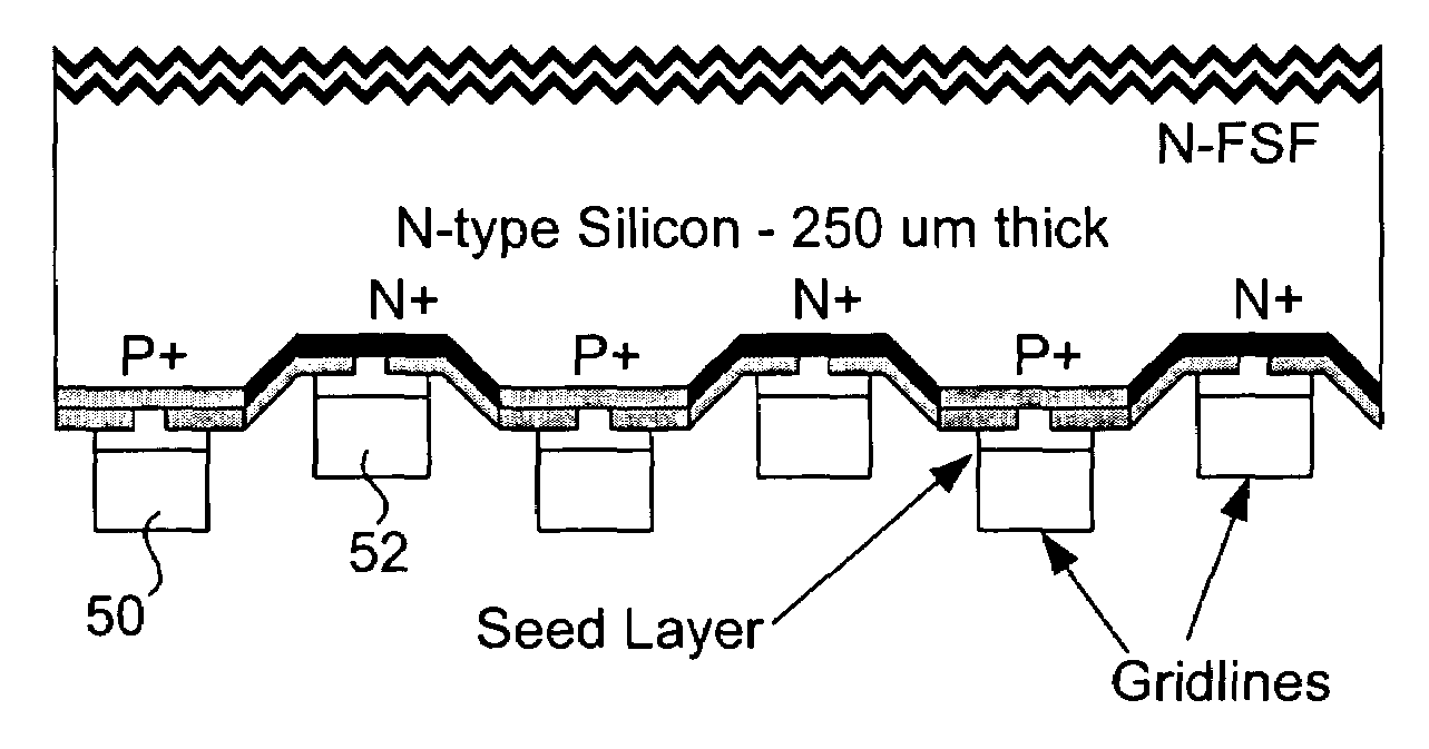
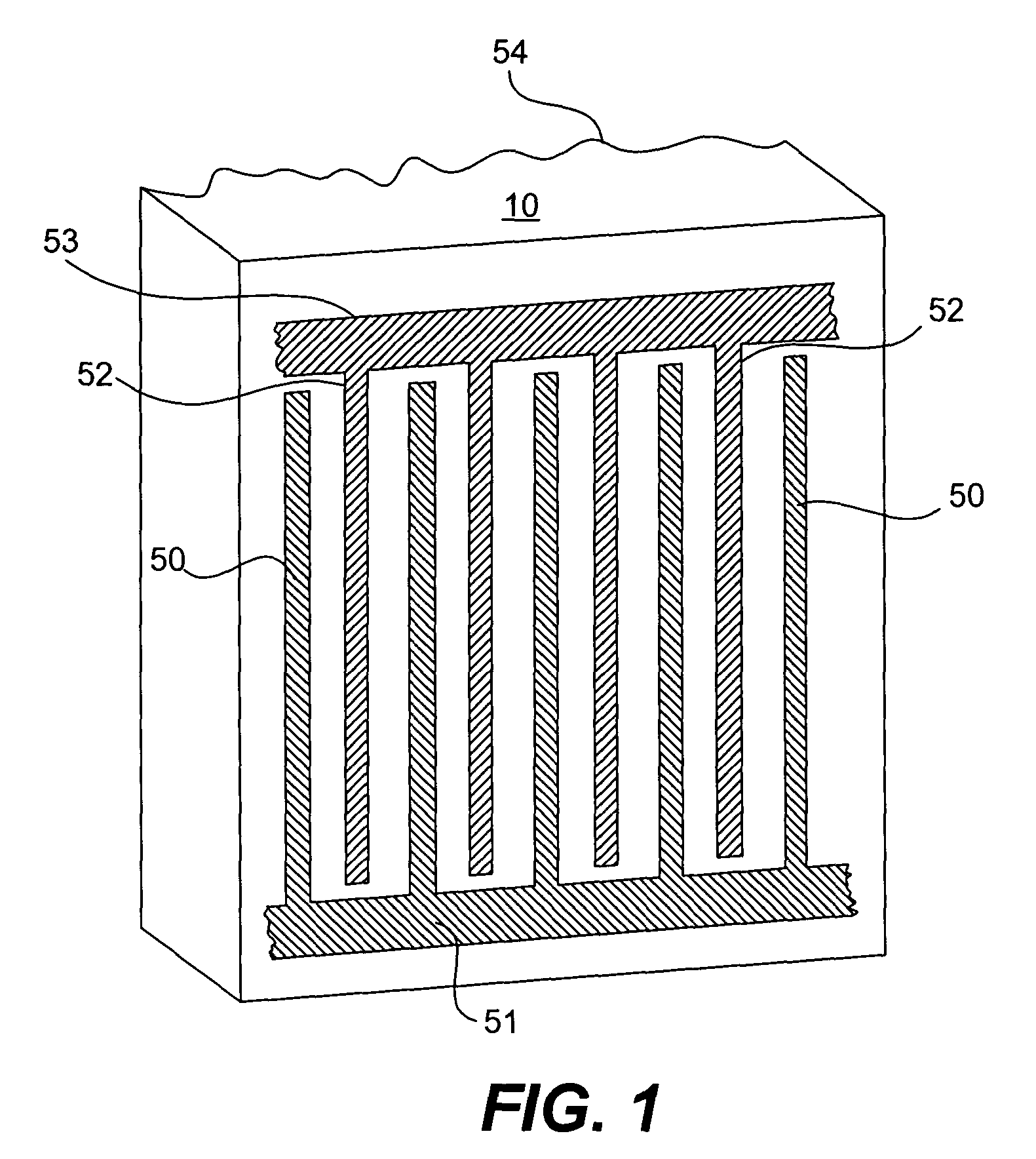
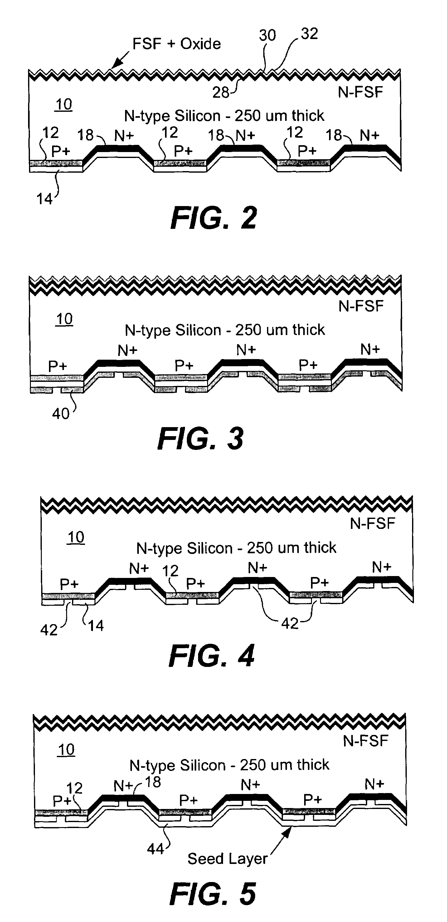
[0011]FIG. 1 is a perspective view of a solar cell in which metal contacts in accordance with the invention are especially applicable. In this embodiment, the cell is preferably manufactured in a single crystalline silicon substrate having a (100) crystalline orientation or in a multi-crystalline silicon substrate with minority carrier lifetime greater than 200 micro-seconds.

[0012]In this embodiment, a front surface of the solar cell has a textured surface 54. An antireflection coating can be applied to assist in the coupling of light energy into the solar cell and improve efficiency. On a back surface, metal contacts 50, 52 in accordance with the invention contact p doped regions and n doped regions respectively, in spaced layers of the back surface. The contacts are respectively connected with grid lines 51, 53 in a grid pattern. The line size is exaggerated in the drawing. The fabrication of the solar cell uses conventional semiconductor processing, including the use of backside ...


PUM

PropertyMeasurementUnit
wavelengthaaaaaaaaaa
electrically conductiveaaaaaaaaaa
chemicalaaaaaaaaaa

Abstract

In a solar cell having p doped regions and n doped regions alternately formed in a surface of a semiconductor wafer in offset levels through use of masking and etching techniques, metal contacts are made to the p regions and n regions by first forming a base layer contacting the p doped regions and n doped regions which functions as an antireflection layer, and then forming a barrier layer, such as titanium tungsten or chromium, and a conductive layer such as copper over the barrier layer. Preferably the conductive layer is a plating layer and the thickness thereof can be increased by plating.

Description

BACKGROUND OF THE INVENTION[0001]This invention relates generally to solar cells, and more particularly the invention relates to metal contact structures for use in solar cells.[0002]The use of photovoltaic cells for the direct conversion of solar radiation into electrical energy is well known, see Swanson, U.S. Pat. No. 4,234,352 for example. Briefly, the photovoltaic cell comprises a substrate of semiconductive material having a p-n junction defined therein. In the planar silicon cell the p-n junction is formed near a surface of the substrate which receives impinging radiation. Radiated photons create mobile carriers (holes and electrons) and the substrate which can be directed to an electrical circuit outside of the cell. Only photons having at least a minimum energy level (e.g., 1.1 electron volt for silicon) can generate an electron-hole pair in the semiconductor pair. Photons having less energy are either not absorbed or are absorbed as heat, and the excess energy of photons h...

Claims


Application Information

Patent Timeline
Patent Type & Authority Patents(United States)
IPC IPC(8): H01L31/00H01L31/0224H01L31/068H01L31/18
CPCH01L31/022441H01L31/0682Y02E10/547
Inventor MULLIGAN, WILLIAM P.CUDZINOVIC, MICHAEL J.PASS, THOMASSMITH, DAVIDSWANSON, RICHARD M.
Owner CREDIT SUISSE CAYMAN ISLANDS BRANCH
Why Eureka
Try Eureka