Subsurface imaging using an electron beam

a technology of electron beam and surface imaging, applied in the direction of material analysis using wave/particle radiation, instruments, etc., can solve the problems of leakage current through the transistor, no easy way to determine exactly where a particular feature of the circuit is, and no information about the impact of the surface ion beam

a technology of electron beam and surface imaging, applied in the direction of material analysis using wave/particle radiation, instruments, etc., can solve the problems of leakage current through the transistor, no easy way to determine exactly where a particular feature of the circuit is, and no information about the impact of the surface ion beam

US7388218B2Active Publication Date: 2008-06-17FEI CO

Image

  • Subsurface imaging using an electron beam
  • Subsurface imaging using an electron beam
  • Subsurface imaging using an electron beam

Examples


Embodiment Construction

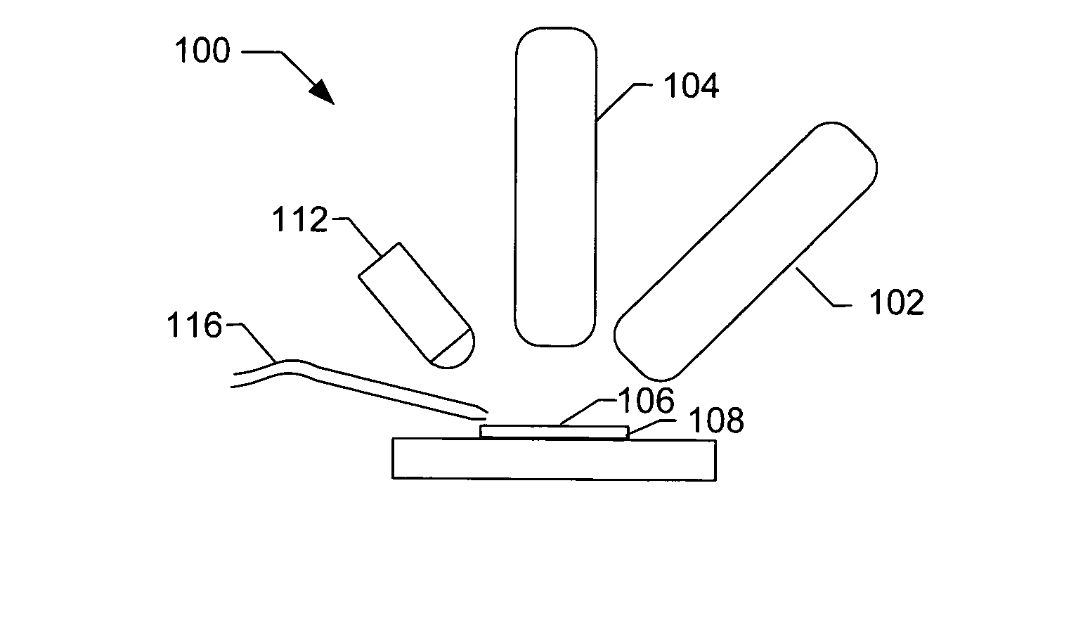
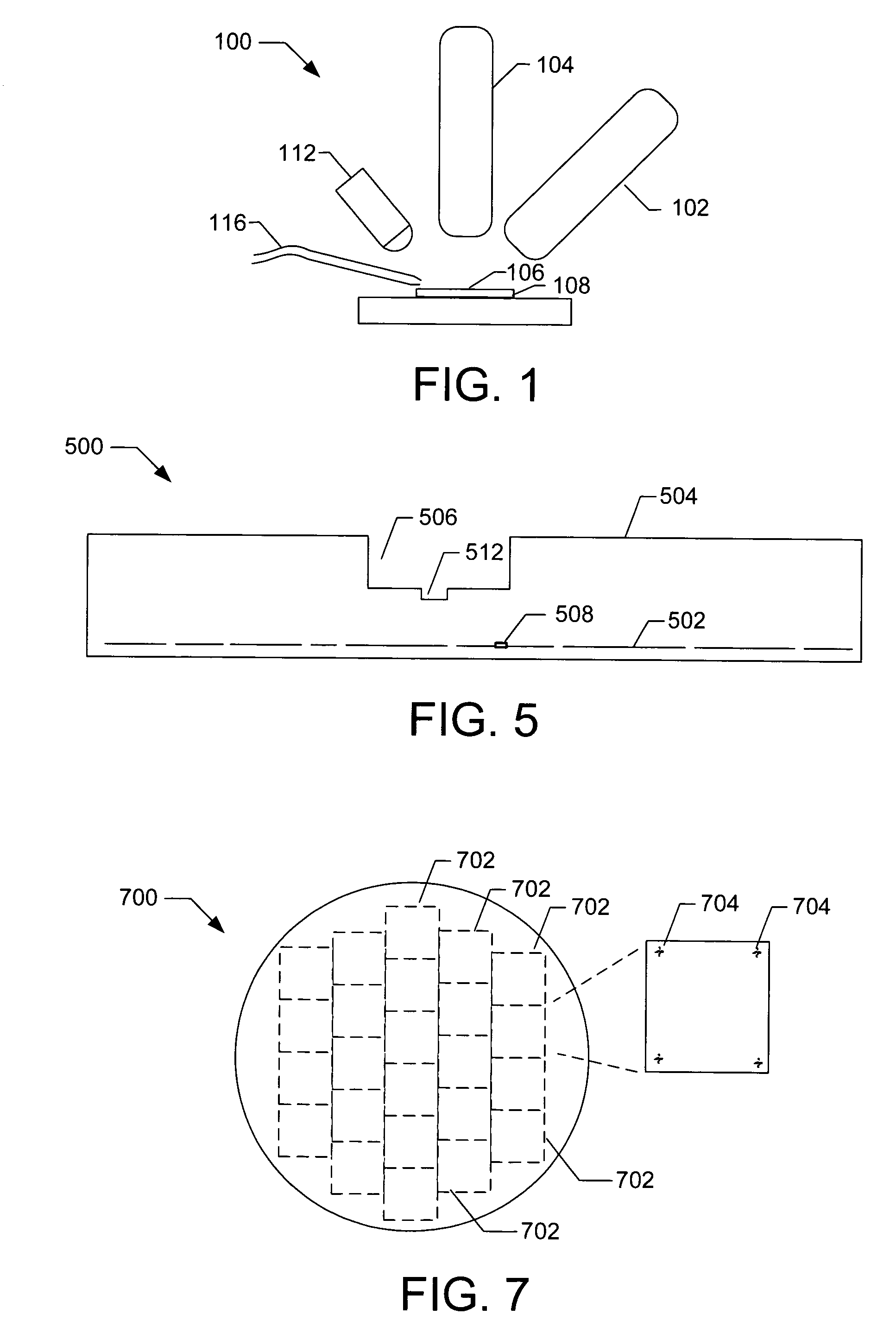
[0025]FIG. 1 shows schematically a dual beam system 100 that is useful for implementing the present invention. One suitable system, for example, is the Model Strata 400 available from FEI Company, the assignee of the present application. The invention can be practiced using any electron beam system having the capability to produce an electron beam having sufficient beam energy, signal detectors, and resolution required for the specific application.

[0026]In the embodiment shown, an electron beam column 102 and an ion beam column 104 are oriented at an angle to each other, and the beams produced by each column impinge on the same spot 106 on a substrate 108. In other embodiments, the impact points are separated, and a stage accurately moves the substrate between the beam impact positions. In such embodiments, the beams can be oriented at an angle to each other to reduce the stage travel distance, or the beams could be parallel. In other embodiments, the ion beam and electron beam can ...


PUM


Abstract

A method of navigating or endpointing a microscopic structure by subsurface imaging using a beam of electrons having sufficient energy to penetrate the surface and produce a subsurface image. For endpointing, when the subsurface image become relatively clear at a known electron energy, a user knows that he is approaching the buried feature. For navigating, a subsurface image can be formed of fiducials or other features to determine the position of the beam on the device.

Description

TECHNICAL FIELD OF THE INVENTION[0001]The present invention relates to methods for navigating, including end pointing, using microscopic features that are buried below the surface of a work piece.BACKGROUND OF THE INVENTION[0002]Modern integrated circuits are composed of multiple layers of conductors, insulators, and semiconductors. Many modern integrated circuits are fabricated using “flip chip” technology in which the circuit is mounted upside-down onto a carrier. To inspect or alter interior layers of such circuits after the chip is mounted, it is necessary to approach the circuit from the backside. Semiconductor wafers are typically several hundred microns thick, so it is necessary to remove a substantial amount of material from the back side of the circuit before reaching the circuit. When accessing circuitry from the backside, there are no reference points for navigation, that is, there is no easy way to determine exactly where a particular feature on the circuit is located. T...

Claims


Application Information

Patent Timeline
17 Jun 2008
Publication
US7388218B2
IPC
H01J49/00
CPC
G01N23/2251; H01J37/304; H01J2237/24592; H01J2237/2817; H01J2237/31
Inventors
CARLESON, PETER D.