Semiconductor device

a technology of semiconductor devices and memory arrays, applied in the field of semiconductor devices, can solve the problems of increasing packaging costs, unable to accurately read or write to storage nodes of two dynamic storage cells, and the degree of shortening of the search time in the search operation of a memory array, which is the heart of the cam, so as to achieve speed-up and reduce power consumption.

Inactive Publication Date: 2008-06-17
PS4 LUXCO SARL
View PDF4 Cites 4 Cited by
  • Summary
  • Abstract
  • Description
  • Claims
  • Application Information

AI Technical Summary

Benefits of technology

[0008]The first problem lies in that the degree of shortening of the search time in the search operation of a memory array, which is the heart of the CAM, is predicted to be small because performance improvement of a semiconductor device is slow in comparison with the line speed which has been improved at a pace as much as 1000 times in 10 years in the communication field where the CAM is primarily applied. Some CAM vendors release on the Web a method to improve the number of searches per unit time by applying several kinds of masks to one search key and carrying out search operations in different look-up tables. However, since a plurality of CAMs are required for carrying out packet transfer processing while maintaining the line speed, there is a possibility that the packaging cost is increased. In order to suppress the packaging cost, parallel processing is desirable, in which search keys sequentially inputted into the CAM are used at different phases to perform the search.
[0030]The effects obtained by typical aspects of the present invention will be briefly described below. It is possible to achieve the speed-up and the reduction in consumption power of a semiconductor device.

Problems solved by technology

The first problem lies in that the degree of shortening of the search time in the search operation of a memory array, which is the heart of the CAM, is predicted to be small because performance improvement of a semiconductor device is slow in comparison with the line speed which has been improved at a pace as much as 1000 times in 10 years in the communication field where the CAM is primarily applied.
However, since a plurality of CAMs are required for carrying out packet transfer processing while maintaining the line speed, there is a possibility that the packaging cost is increased.
However, in the folded bit-line structure, information of a logical value “00” or a logical value “11” cannot be accurately read from or written to storage nodes of the two dynamic storage cells.
Furthermore, in the case of dynamic cells, re-store operation for refresh cannot be correctly carried out.
Furthermore, since a search-line driver has a structure to generate complementary signals to search line pairs in patent document 1, it is impossible to carry out the search operation in which a mask is applied to optional bits of a search key and the corresponding bits are forcibly regarded as the matched bits.

Method used


Image

  • Semiconductor device
  • Semiconductor device
  • Semiconductor device

Examples


first embodiment

[0049]First, the entire structure of a CAM will be described.

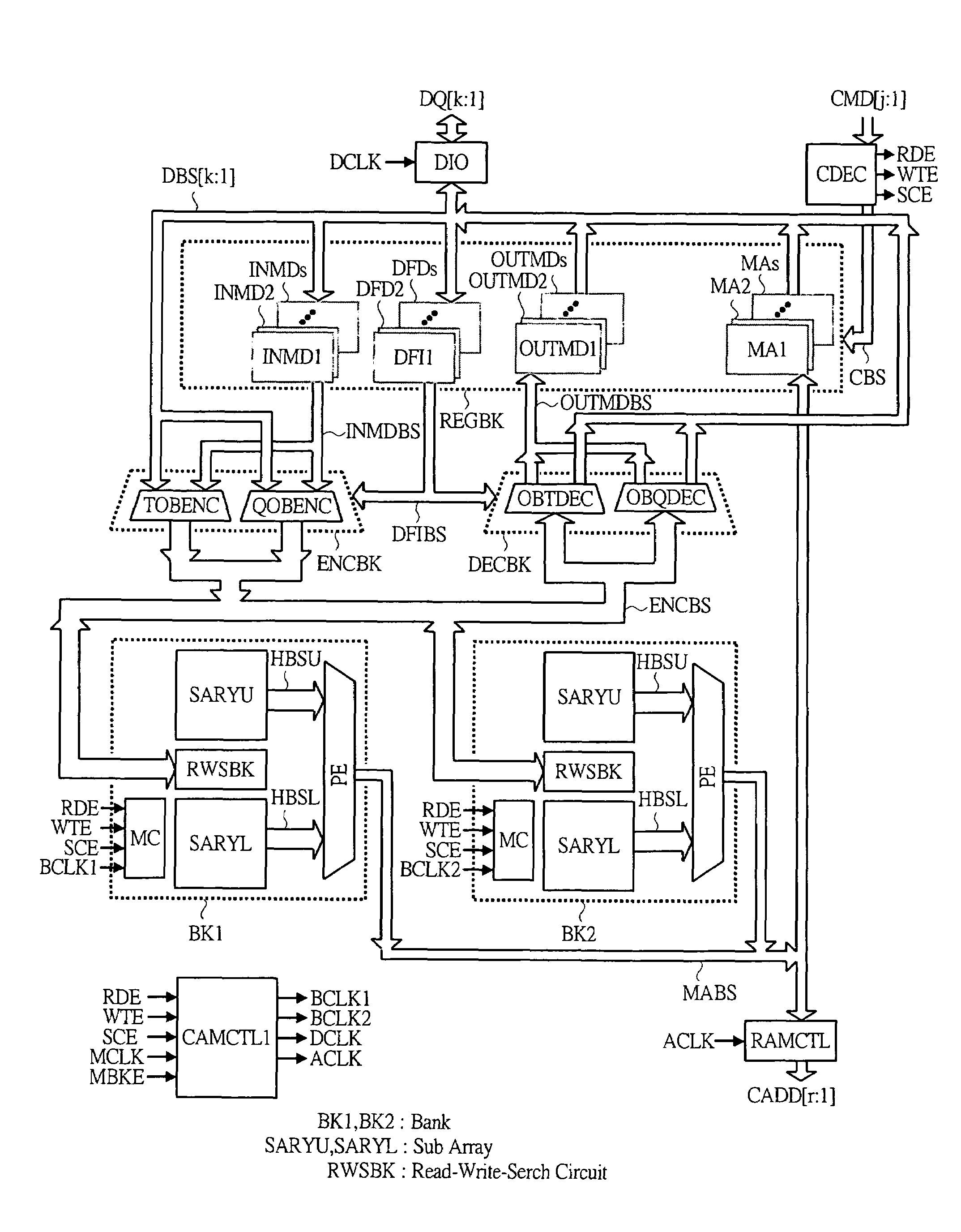
[0050]FIG. 1 is a block diagram showing an example of a basic structure of principal blocks of a CAM included in the semiconductor device according to the first embodiment of the present invention. This structure includes a command decoder CDEC, a CAM control circuit CAMCTL1, a data I / O circuit DIO, various register blocks REGBK, an encoder block ENCBK, a decoder block DECBK, banked memory arrays BK1 and BK2, and a RAM control circuit RAMCTL. In FIG. 1, attention is placed on the path in which the data in search operation is transmitted and received, and a refresh counter, a low decoder, and others which are address-related circuit blocks are omitted for simplicity.

[0051]The command decoder CDEC receives and encodes command signals CMD [j:1] and outputs signals for selecting a register described later to various register blocks REGBK via a command bus CBS. Alternatively, it outputs a read enable signal RDE, a write enable ...

second embodiment

[0104]In the second embodiment, another example of the structure and the operation of the CAM described in the first embodiment will be described.

[0105]FIG. 8 is a block diagram showing an example of the basic structure of principal blocks of the CAM included in a semiconductor device according to the second embodiment of the present invention. The features of this structure lie in that banked memory arrays form a hierarchical structure, and the search operation of search keys wider than the bus width of the data bus DQ is performed by using a memory array structure which has two main banks composed of multiple banks. In the following description, the structure of FIG. 8 will be described while focusing on the points different from the structure shown in FIG. 1.

[0106]A CAM control circuit CAMCTL8 receives a master clock MCLK and a multi bank enable signal MBKE generated by a controller (or a control circuit called network processor or search engine, etc.) connected to the CAM accord...

third embodiment

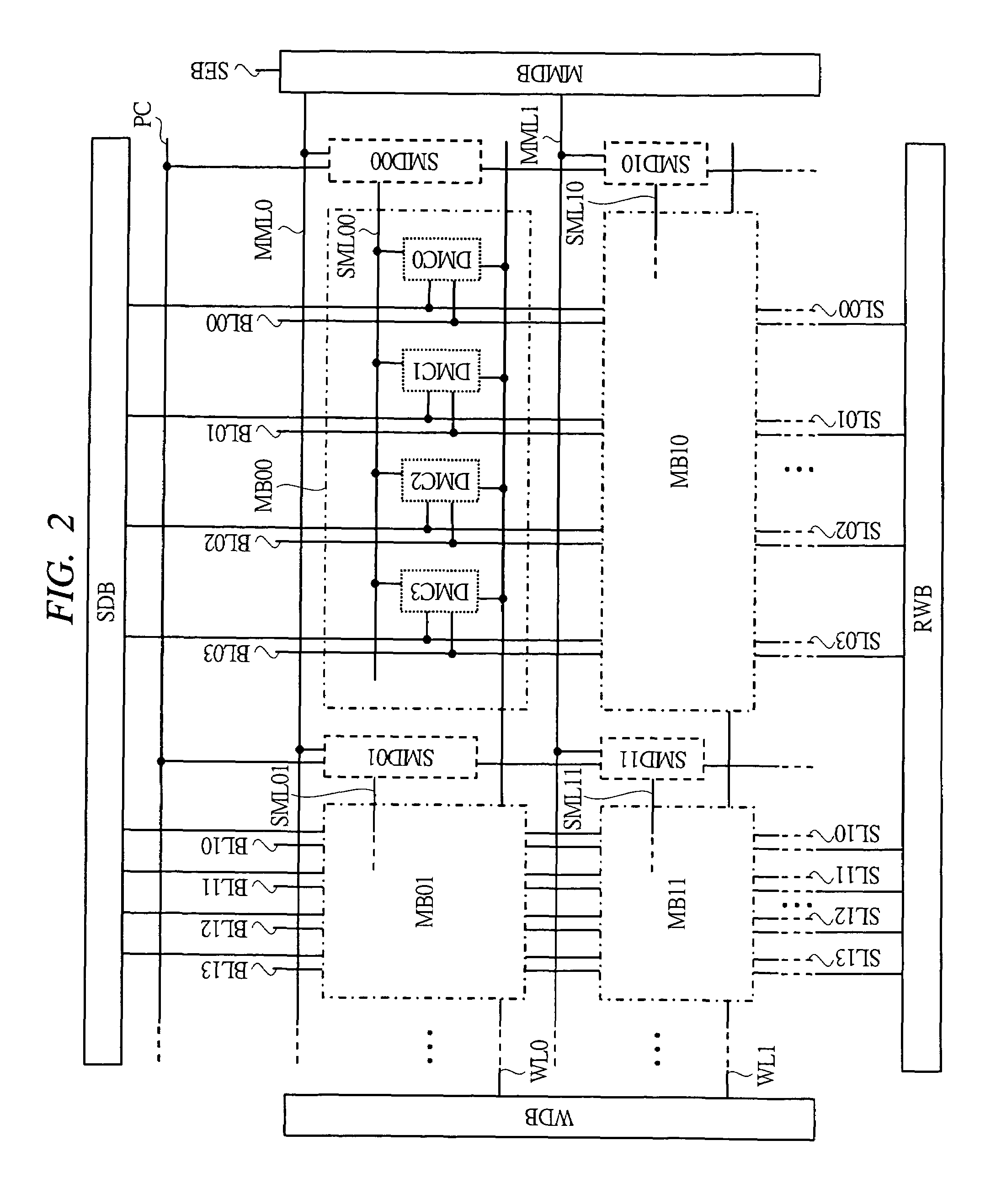
[0130]In the third embodiment, another example of the structure and the operation of the sub-array used in the CAM described in the first and second embodiments will be described. FIG. 11 is a circuit block diagram showing an example of a memory array structure different from that of FIG. 2 in the CAM included in a semiconductor device according to the third embodiment of the present invention. In the following description, the structure of FIG. 11 will be described while focusing on the points different from the memory array structure shown in FIG. 2.

[0131]The features of the memory array structure shown in FIG. 11 lie in that, in addition to normal memory blocks shown in FIG. 2 and FIG. 3, dummy memory blocks MBD0, MBD1, . . . with the same structure are further disposed on a dummy word line WLD to generate the sense amplifier start timing. Between dummy sub-match lines SMLD0, SMLD1, . . . and a dummy main match line MMLD in the dummy memory blocks MBD0, MBD1, . . . , correspondin...


PUM


Abstract

Control clocks of different phases are distributed to a memory array divided into multiple banks, and processing of entries and search keys (read and write operations and search operation) is performed at different phases. The memory array divided into banks is further divided into smaller arrays, that is, sub-arrays, and a sense amplifier in a read-write-search circuit block is shared by the two sub-arrays. In this case, a so-called open bit line structure in which each one bit line is connected from both sub-arrays to a sense amplifier is adopted. The same look-up table is registered to multiple banks, successively inputted search keys are sequentially inputted to the multiple banks, and the search operation is carried out in synchronization with the control clocks of different phases.

Description

CROSS-REFERENCE TO RELATED APPLICATION[0001]The present application claims priority from Japanese Patent Application No. JP 2005-040885 filed on Feb. 17, 2005, the content of which is hereby incorporated by reference into this application.TECHNICAL FIELD OF THE INVENTION[0002]The Present invention relates to a semiconductor device. More particularly, it relates to a technology effectively applied to a semiconductor device provided with a content addressable memory (CAM) array which stores and compares information encoded in the device, in a semiconductor device including a content addressable memory cell (CAM cell) which compares information stored in a storage node with inputted information.BACKGROUND OF THE INVENTION[0003]With the explosive growth of the Internet, the table scale required for routers and switches in a network has been rapidly increasing, and the speed-up of table search has been demanded. As means for solving this problem from the aspect of hardware, a ternary con...

Claims


Application Information

Patent Timeline
Patent Type & Authority Patents(United States)
IPC IPC(8): G11C15/00
CPCG11C15/04G11C15/043
Inventor HANZAWA, SATORUTAKEMURA, RIICHIROKAJIGAYA, KAZUHIKO
Owner PS4 LUXCO SARL
Why Eureka
Try Eureka