Laser process apparatus, laser irradiation method, and method for manufacturing semiconductor device

a technology of laser irradiation and process equipment, which is applied in the direction of recording equipment, manufacturing tools, instruments, etc., can solve the problems of easy deformation and inferior heat resistance of glass substrate, and achieve the effects of reducing vibration generation, high reliability, and suppressing vibration generation

Inactive Publication Date: 2008-06-24
SEMICON ENERGY LAB CO LTD
View PDF23 Cites 4 Cited by
  • Summary
  • Abstract
  • Description
  • Claims
  • Application Information

AI Technical Summary

Benefits of technology

[0049]According to the present invention, the acceleration of the scanning speed of the substrate at the laser irradiation is kept almost constant, and the generation of vibration can be suppressed to the minimum.
[0050]Moreover, since the substrate is scanned in one direction at the laser irradiation, a semiconductor film can be irradiated with a homogeneous laser beam, thereby homogenizing the effect of the laser annealing.
[0051]Moreover, according to the present invention, a large substrate can be annealed by a laser at one time, and many substrates can be processed at one time.
[0052]Therefore, the present invention can provide a laser process apparatus which can decrease the generation of vibration and which can process many substrates at one time. This makes it possible to mass-produce semiconductor devices with high reliability in short time.

Problems solved by technology

The glass substrate is inferior in heat resistance and easy to be deformed due to heat.

Method used


Image

  • Laser process apparatus, laser irradiation method, and method for manufacturing semiconductor device
  • Laser process apparatus, laser irradiation method, and method for manufacturing semiconductor device
  • Laser process apparatus, laser irradiation method, and method for manufacturing semiconductor device

Examples


embodiment mode 1

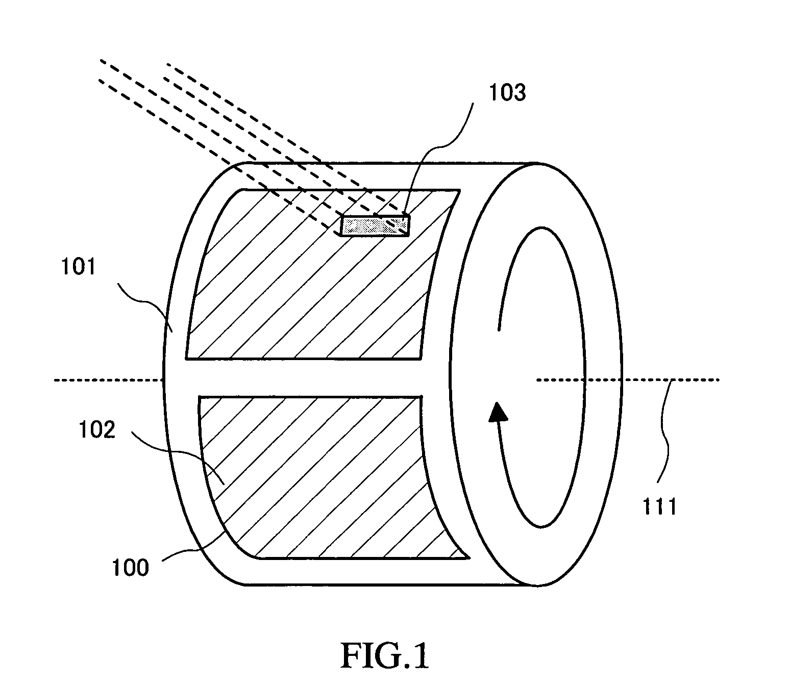
[0053]A specific apparatus structure of the present invention is described with reference to FIG. 1. It is to be noted that the same things as what has already been described in “Means for Solving the Problems” are shown with the same reference numerals. However, since the present invention can be carried out with many different modes, it is to be understood by those skilled in the art that the mode and the detail can be changed variously without departing from the spirit and the scope of the present invention. Therefore, the present invention is not construed as being limited to the description of the present embodiment mode.

[0054]Since the thickness of the substrate 100, for example a large glass substrate, used in this embodiment mode is as thin as 1 mm or less, the curvature can be given comparatively easily. For example, a curvature of a radius of curvature of 1 m can be easily given to a glass substrate having a size of 600×720 mm and a thickness of 0.7 mm.

[0055]Consequently, ...

embodiment mode 2

[0060]An embodiment mode of the present invention is described with reference to FIG. 2 and FIG. 25. However, since the present invention can be carried out with many different modes, it is to be understood by those skilled in the art that the mode and the detail can be changed variously without departing from the spirit and the scope of the present invention. Therefore, the present invention is not construed as being limited to the description of this embodiment mode.

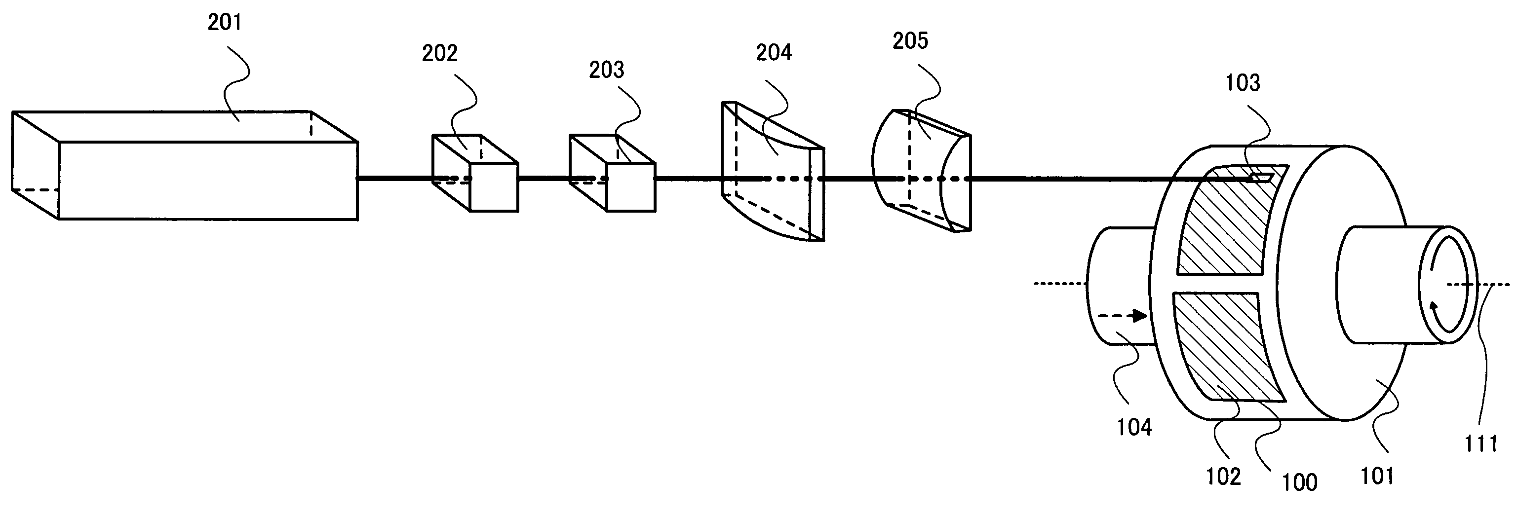
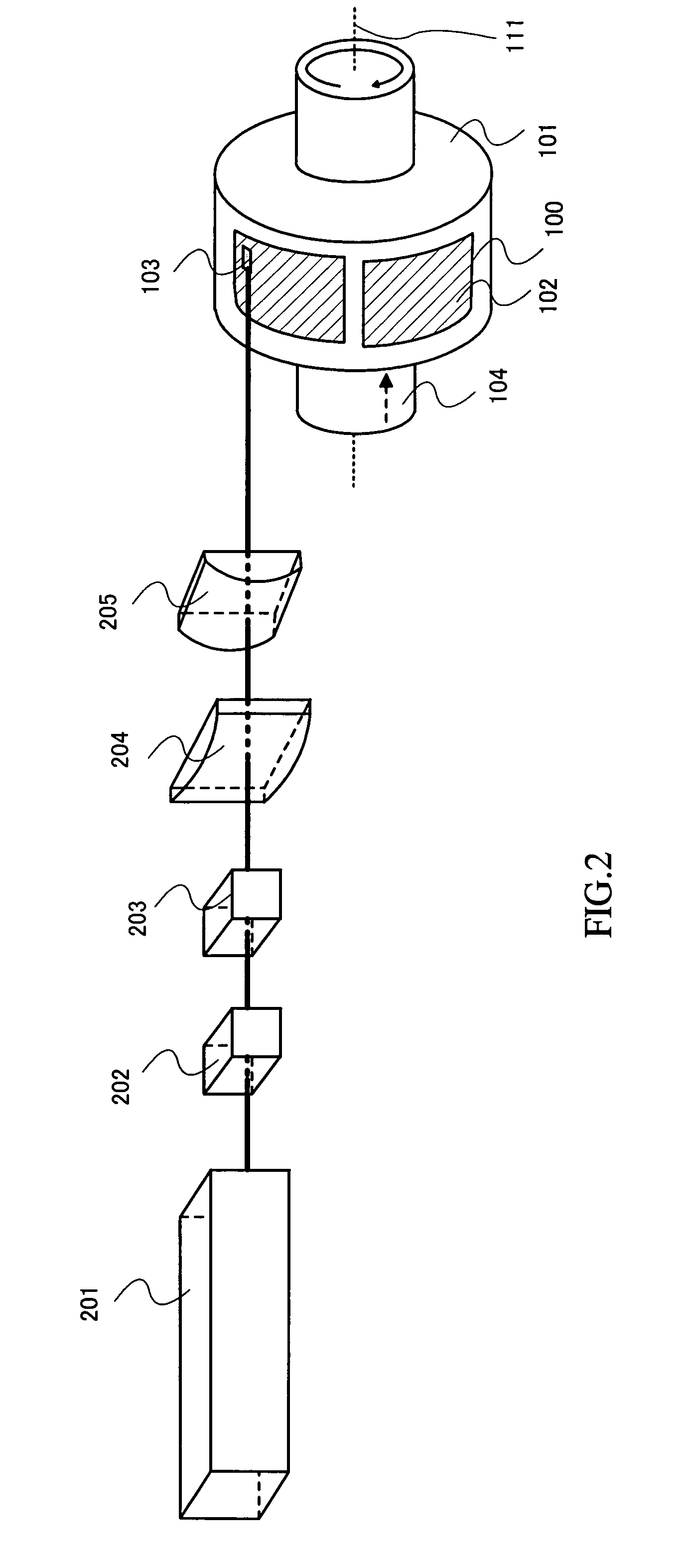
[0061]In this embodiment, a laser process apparatus shown in FIG. 2 has a laser oscillator 201, a beam expander 202, a beam homogenizer 203, and an optical system including cylindrical lenses 204 and 205.

[0062]In FIG. 2, a laser beam emitted from the CW laser oscillator 201 having an output of 10 W and a wavelength of 532 nm enters the beam expander 202 so that the beam diameter is expanded, and then enters the beam homogenizer 203. The beam homogenizer 203 has a role for homogenizing the intensity distribution of the ...

embodiment mode 3

[0073]This embodiment mode is described with reference to FIG. 3 and FIG. 4. In this embodiment mode, laser irradiation is conducted by a plurality of laser beams. This can process more substrates at one time, which increases the productivity.

[0074]In FIG. 3 and FIG. 4, the same things as those in Embodiment Modes 1 and 2 are shown with the same reference numerals.

[0075]However, since the present invention can be carried out with many different modes, it is to be understood by those skilled in the art that the mode and the detail can be changed variously without departing from the spirit and the scope of the present invention. Therefore, the present invention is not construed as being limited to the description of this embodiment mode.

[0076]In this embodiment mode, a laser process apparatus shown in FIG. 4 has a laser oscillator 201a, a beam expander 202a, a beam homogenizer 203a, an optical system A (210a) including cylindrical lenses 204a and 205a, a laser oscillator 201b, a beam ...


PUM

PropertyMeasurementUnit
speedaaaaaaaaaa
thicknessaaaaaaaaaa
thicknessaaaaaaaaaa

Abstract

To mass-produce semiconductor devices with high reliability in short time by suppressing the generation of vibration at the laser irradiation and moving a laser beam having homogeneous energy profile in one direction.A substrate is sucked onto a surface of a cylindrical rotator along the curvature of the rotator, the rotator is rotated, and a semiconductor film formed over the substrate is irradiated with a laser at one time. Moreover, a moving mechanism is provided in a rotational axis direction of the rotator, and an irradiation position is displaced at each rotation of the rotator. Alternatively, the irradiation position can be moved in the rotational axis direction while rotating the rotator.

Description

TECHNICAL FIELD[0001]The present invention relates to a laser beam irradiation method and a laser process apparatus for conducting it. Further, the present invention relates to a method for manufacturing a semiconductor device by using the laser beam irradiation.BACKGROUND ART[0002]In recent years, a technique to manufacture a thin film transistor (Thin Film Transistor, hereinafter referred to as a “TFT”) over a substrate has made great progress and application development to, for example, an active matrix display device has been advanced. In particular, a TFT formed using a crystalline semiconductor film is superior in field-effect mobility (also referred to as mobility) to a TFT formed using a conventional amorphous semiconductor film; therefore, high-speed operation is possible. For this reason, it is tried that a pixel, which has been controlled by a driver circuit provided outside a substrate, is controlled by a driver circuit formed over the same substrate as the pixel.[0003]A...

Claims


Application Information

Patent Timeline
Patent Type & Authority Patents(United States)
IPC IPC(8): H01L21/84B23K26/08H01L21/00H01L21/20H01L21/77H01L27/12
CPCB23K26/0823H01L27/1285H01L27/1266H01L27/12H01L21/2026H01L21/02683H01L21/02502H01L21/02488H01L21/02422H01L21/02505H01L21/0242H01L21/02686H01L21/02532H01L21/0245H01L21/02595H01L21/02513H01L21/02691H01L21/02678
Inventor TANAKA, KOICHIRO
Owner SEMICON ENERGY LAB CO LTD
Why Eureka
Try Eureka