Semiconductor structure including silicide regions and method of making same

a technology of silicide region and semiconductor structure, which is applied in the direction of semiconductor devices, basic electric elements, electrical equipment, etc., can solve the problems of low reliability, and high junction leakage curren

Active Publication Date: 2008-07-08
TAIWAN SEMICON MFG CO LTD
View PDF53 Cites 33 Cited by
  • Summary
  • Abstract
  • Description
  • Claims
  • Application Information

AI Technical Summary

Benefits of technology

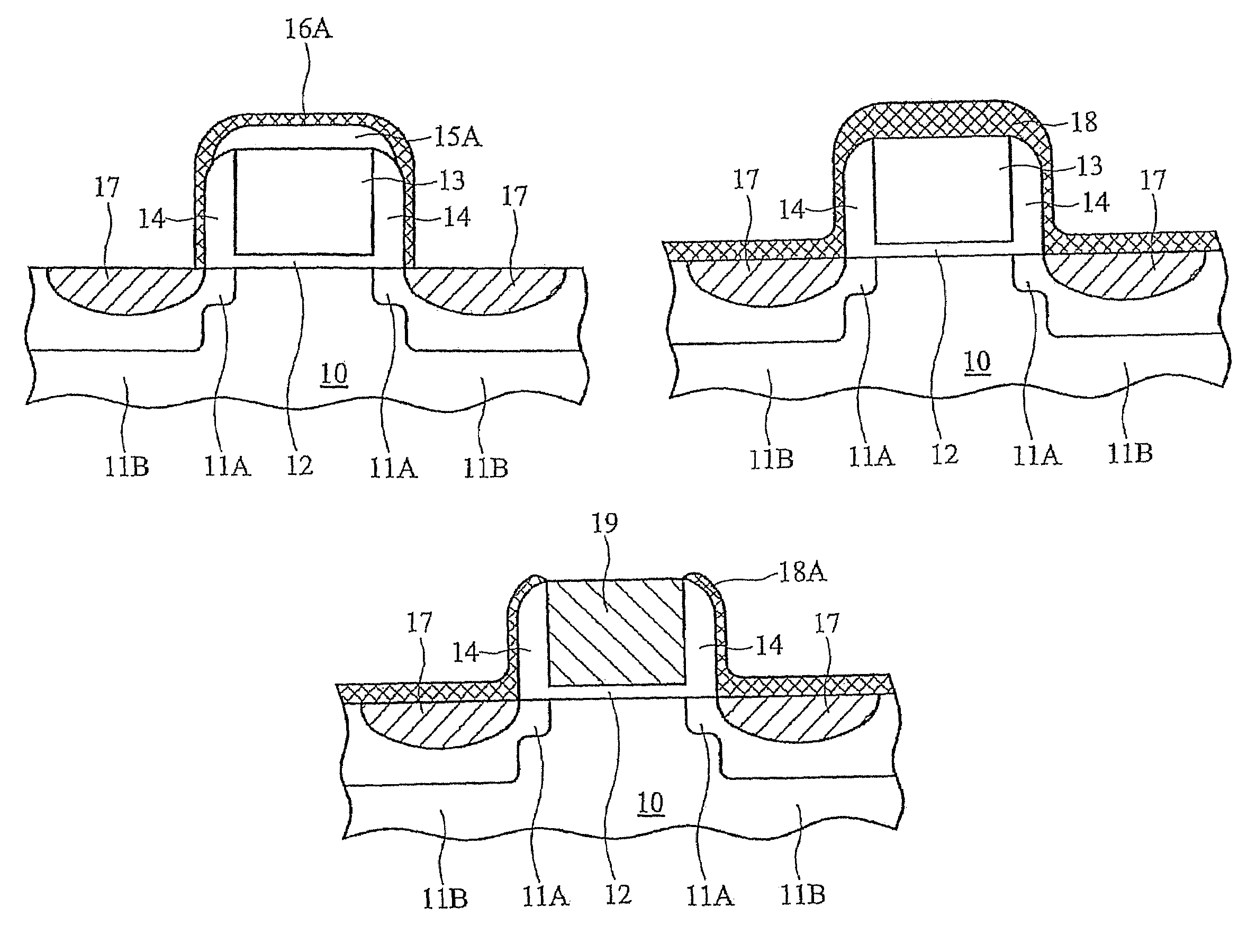
[0023]The manufacturing process described herein is adaptable to manufacturing any of the various types of semiconductor devices, particularly advanced deep-submicron CMOS devices, such as 0.1 micron devices with ultra-shallow junctions, e.g., above 500 Å to about 2000 Å, while significantly improving the reliability of ultra-shallow junctions. Reduction of parasitic, sheet and contact resistance between the active regions and the gate electrode and interconnects may be achieved without increasing junction leakage current. Greater control of the silicidation process is provided in forming fully or partially silicided gate electrode 19 and silicided active regions 17, without compromising the reliability of the active regions. Therefore, improved fully silicided gates may be achieved along with consequent benefits thereof, such as lower gate electrode resistance, improved device speed, prevention or reduction of boron migration into the gate electrode and reduction or elimination of the depletion effect, without high junction leakage current or spiking.

Problems solved by technology

The formation of a thick silicide layer, however, may cause a high junction leakage current and low reliability, particularly when forming ultra-shallow junctions.
The formation of a thick silicide layer consumes silicon from the underlying semiconductor substrate such that the thick silicide layer approaches and even shorts the ultra-shallow junction, thereby generating a high junction leakage current.
However, formation of silicide on the gate electrode simultaneously with the source / drain regions leads to the risk of spiking in the source / drain regions if the complete or nearly complete silicidation of the gate electrode is attempted.
This process, therefore, suffers from a very narrow process window due to the strong likelihood that exposure of the metal and silicon to rapid thermal annealing conditions sufficient to completely silicidize a gate electrode will also cause the silicide in the source / drain region to spike and reach the bottom of the junction, undesirably causing leakage.

Method used


Image

  • Semiconductor structure including silicide regions and method of making same
  • Semiconductor structure including silicide regions and method of making same
  • Semiconductor structure including silicide regions and method of making same

Examples


Embodiment Construction

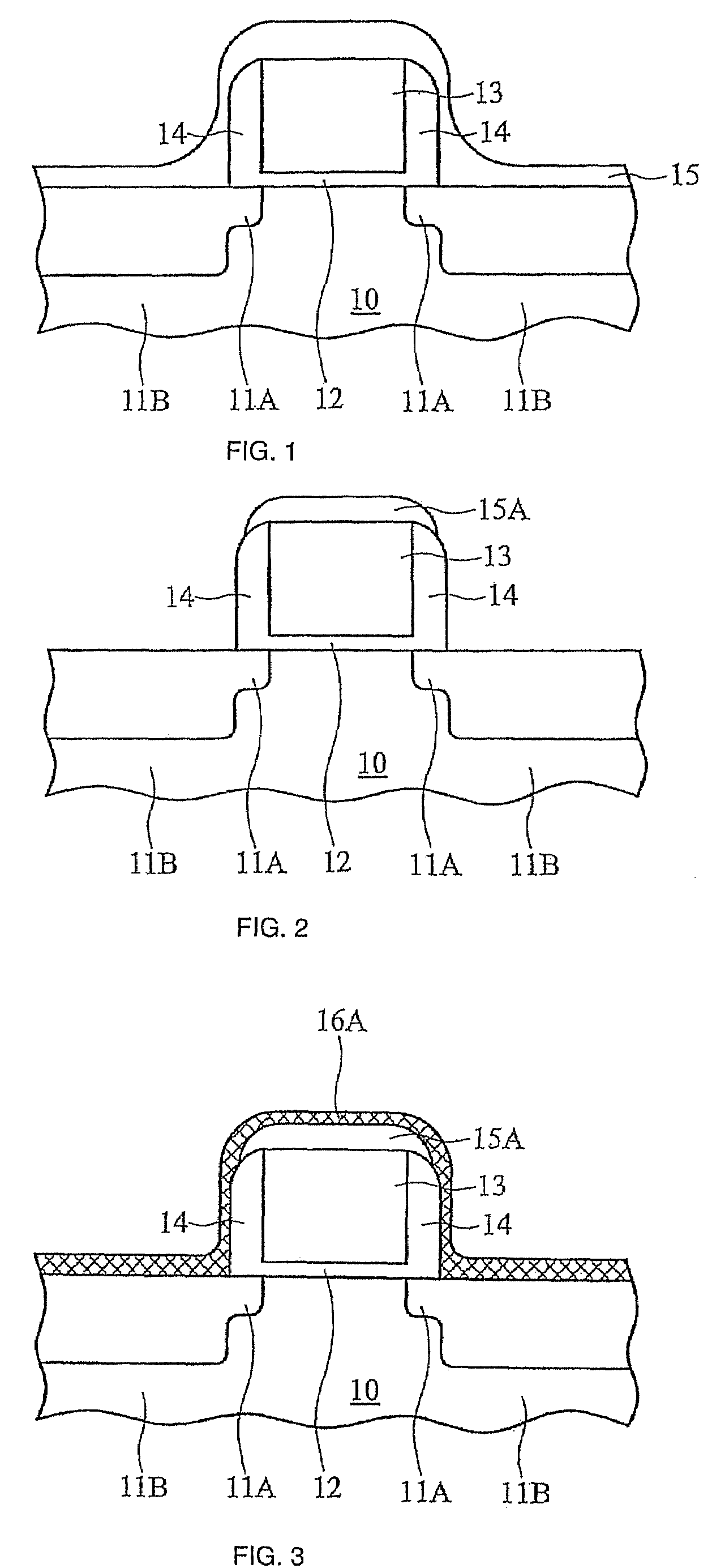
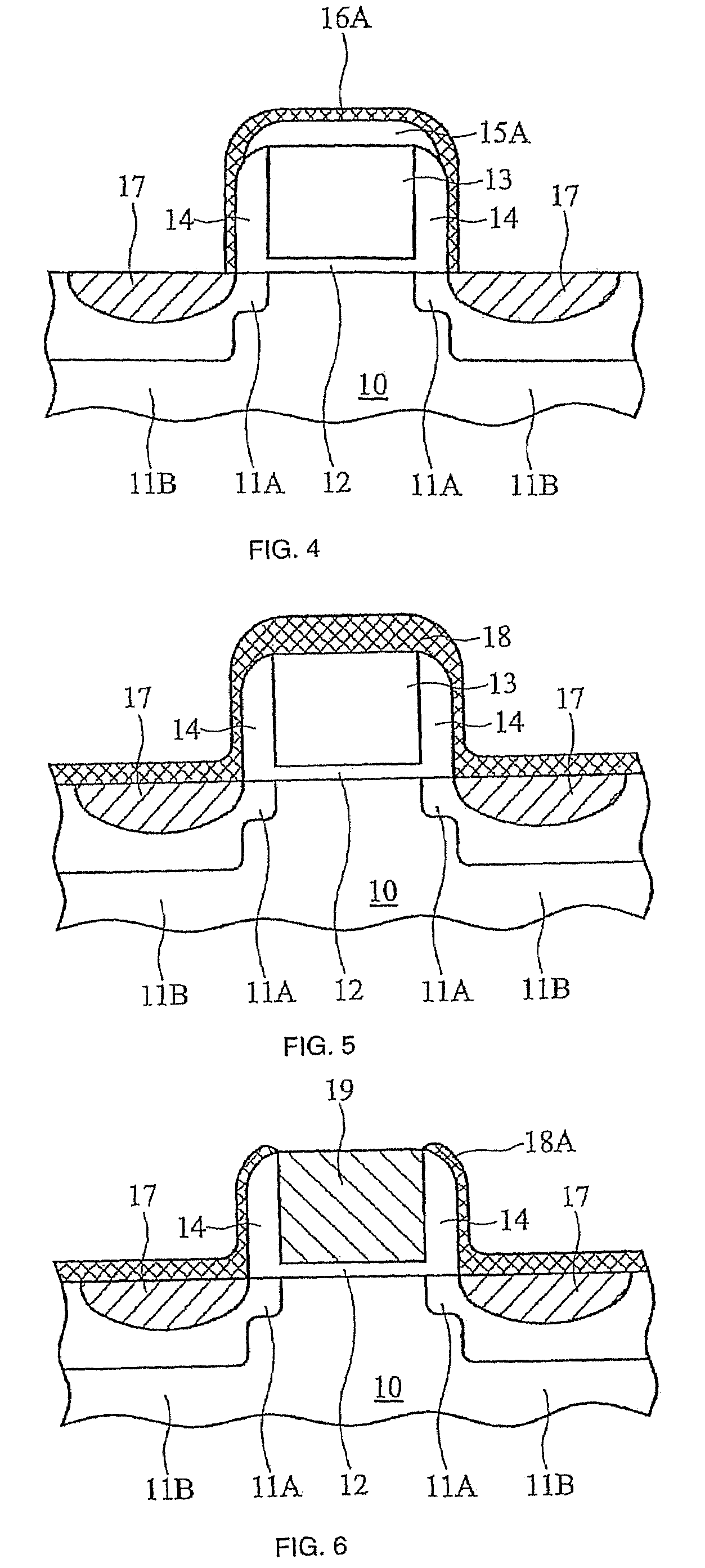
[0011]The method steps described below do not form a complete process flow for manufacturing integrated circuits. The present embodiments can be practiced in conjunction with integrated circuit fabrication techniques currently used in the art, and only so much of the commonly practiced process steps are included as are necessary for an understanding of the described embodiments. The figures represent cross-section portions of a semiconductor chip or a substrate during fabrication and are not drawn to scale, but instead are drawn to illustrate the features of the described embodiments.

[0012]Sequential steps of an exemplary embodiment of the method of forming silicide regions in a semiconductor substrate are described below with respect to the schematic illustrations of FIGS. 1-7. Similar reference numerals denote similar features. Referring first to FIG. 1, a conventional transistor structure is shown comprising a substrate 10 doped with either an N-type impurity or P-type impurity, ...


PUM

PropertyMeasurementUnit
temperatureaaaaaaaaaa

Abstract

A method of forming a silicided gate on a substrate having active regions, comprising the steps of: forming a first silicide in the active regions from a first material; and forming a second silicide in the gate from a second material, wherein the first silicide forms a barrier against the second material forming a silicide in the active regions during the second silicide forming step, wherein said second silicide is thicker than said first silicide.

Description

FIELD OF THE INVENTION[0001]The present invention relates to semiconductor fabrication and more particularly to methods of forming field effect transistors having silicided regions.BACKGROUND OF THE INVENTION[0002]The principle way of reducing contact resistance between polysilicon gates and source / drain regions and interconnect lines is by forming a metal silicide atop the source / drain regions and the gate electrodes prior to application of the conductive film for formation of the various conductive interconnect lines. Presently, the most common metal silicide materials are CoSi2 and TiSi2, typically formed by the so called salicide (self-aligned silicide) process. In the salicide process, a thin layer of a metal, such as titanium, is blanket deposited over the semiconductor substrate, specifically over exposed source / drain and gate electrode regions. The wafer is then subjected to one or more annealing steps, for example at a temperature of 800° C. or higher for titanium. This ann...

Claims


Application Information

Patent Timeline
Patent Type & Authority Patents(United States)
IPC IPC(8): H01L21/44H01L21/28H01L21/336H01L29/45H01L29/49
CPCH01L21/28097H01L29/66507H01L29/4908H01L29/458
Inventor WU, CHII-MINGLIN, CHENG-TUNGWANG, MEI-YUNCHANG, CHIH-WEISHUE, SHAU-LIN
Owner TAIWAN SEMICON MFG CO LTD
Why Eureka
Try Eureka