Semiconductor-on-insulator (SOI) structures including gradient nitrided buried oxide (BOX)

a technology of buried oxide and semiconductor devices, applied in the field of semiconductor devices, can solve the problems of narrow width effect, impact on the threshold voltage of semiconductor devices, and the impact of boron migration and segregation may be even more sever

Active Publication Date: 2008-07-08
META PLATFORMS INC
View PDF14 Cites 7 Cited by
  • Summary
  • Abstract
  • Description
  • Claims
  • Application Information

AI Technical Summary

Problems solved by technology

For example, the migration and segregation of boron to oxide isolation regions may cause narrow width effects in semiconductor channels which in turn may impact a semiconductor device threshold voltage.
Within the context of devices fabricated within semiconductor-on-insulator (SOI) structures, the impact of boron migration and segregation may be even more severe since there is typically also a buried oxide interface located below a semiconductor device.
A massive loss of boron into an underlying buried oxide (BOX) layer may lead to a high parasitic resistance and a compromised semiconductor device performance.
A potential solution to boron migration might be the use of a laser or flash anneal process for boron activation, but this solution severely restricts the process flow, and requires that a boron dopant in a semiconductor-on-insulator (SOI) structure never be exposed to a conventional spike anneal once the boron dopant is in place.
This solution may lead to increased complexity in device integration, and to added constrains in device design.
In general, one of the drawbacks of the SIMOX process is a high back-interface charge at the oxide / Si interface.
The presence of back interface charge can lead to mobility degradation (and hence reduced drive current) in the channel of CMOS transistors fabricated on SIMOX substrates.
The degradation is especially severe in CMOS devices fabricated on SIMOX substrates where the active Si layer is thin (<20 nm) as is the case for fully-depleted CMOS fabricated on ultra-thin SOI.

Method used


Image

  • Semiconductor-on-insulator (SOI) structures including gradient nitrided buried oxide (BOX)
  • Semiconductor-on-insulator (SOI) structures including gradient nitrided buried oxide (BOX)
  • Semiconductor-on-insulator (SOI) structures including gradient nitrided buried oxide (BOX)

Examples


first embodiment

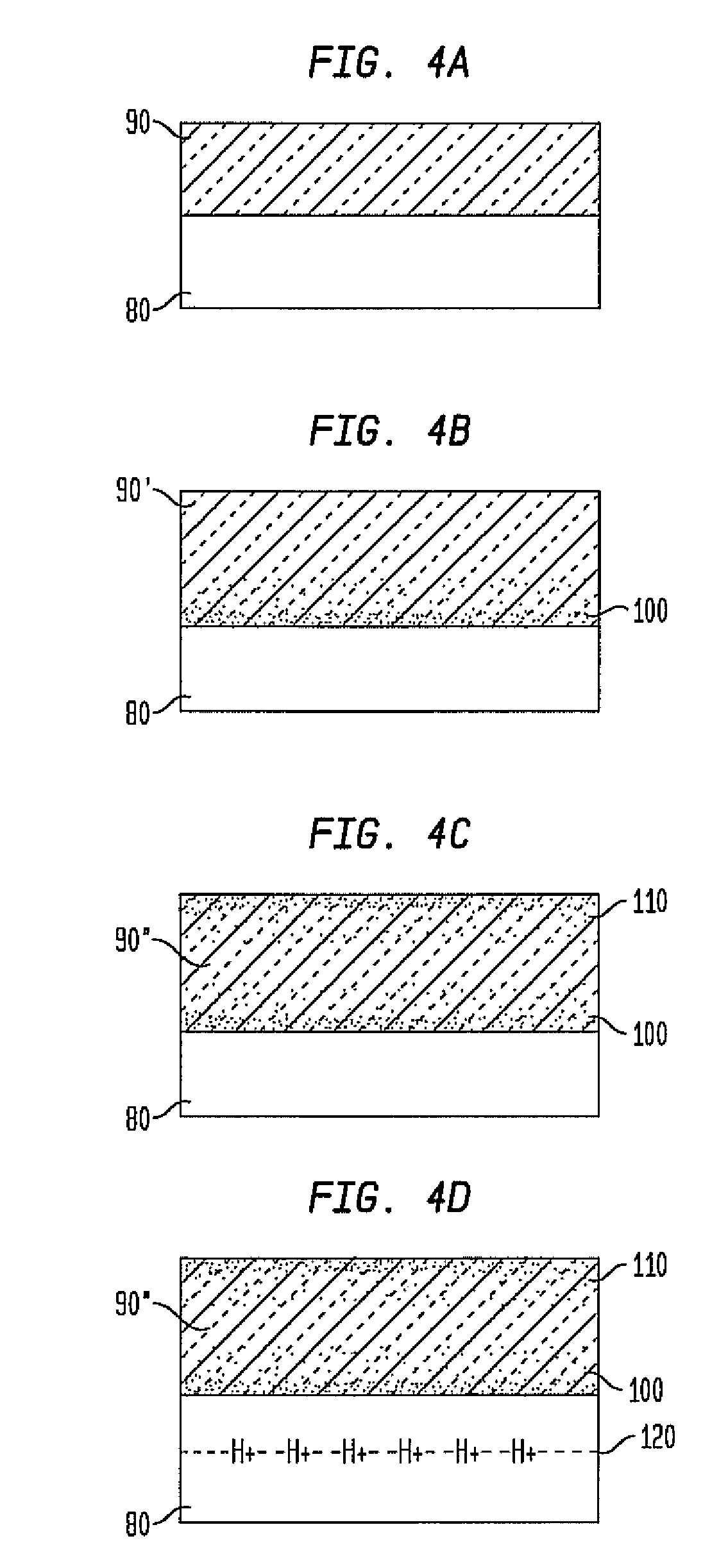
[0032]FIG. 4A to FIG. 4F show a series of schematic cross-sectional diagrams illustrating the results of progressive stages in fabricating a semiconductor-on-insulator (SOI) structure in accordance with an embodiment of the invention. This embodiment of the invention comprises the invention.

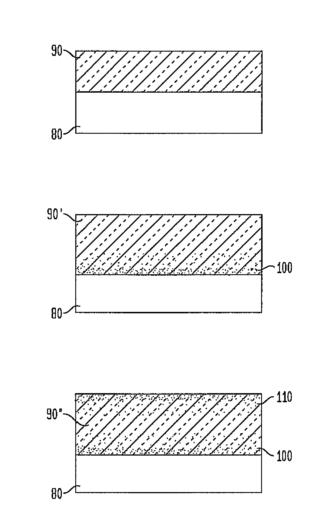
[0033]FIG. 4A shows a semiconductor substrate 80. A buried oxide (BOX) layer 90 is located upon the semiconductor substrate 80.

[0034]The semiconductor substrate 80 may comprise any of several semiconductor materials. Non-limiting examples include silicon, germanium, silicon-germanium alloy, silicon carbide, silicon-germanium carbide alloy and compound semiconductor materials. Non-limiting examples of compound semiconductor materials include gallium arsenide, indium arsenide and indium phosphide semiconductor materials. Typically, the semiconductor substrate 80 comprises a silicon or silicon-germanium alloy semiconductor material that has a thickness from about 1 to about 3 mm.

[0035]The buried oxi...

second embodiment

[0048]FIG. 5A and FIG. 5B show a pair of schematic cross-sectional diagrams illustrating the results of progressive stages in fabricating a semiconductor-on-insulator (SOI) structure in accordance with another embodiment of the invention. This other embodiment of the invention comprises the invention.

[0049]FIG. 5A shows a schematic cross-sectional diagram of a semiconductor-on-insulator (SOI) structure generally related to the first embodiment. The semiconductor-on-insulator (SOI) structure in accordance with the second embodiment results from further processing of the semiconductor-on-insulator (SOI) structure of FIG. 4C within the first embodiment.

[0050]The semiconductor-on-insulator (SOI) structure of the second embodiment that is illustrated in FIG. 5A comprises, in a first instance, the semiconductor substrate 80 that comprises a base semiconductor substrate. The buried oxide (BOX) layer 90″ further comprising the first nitrogen gradient 100 and the second nitrogen gradient 110...


PUM


Abstract

A semiconductor-on-insulator structure includes a buried dielectric layer interposed between a base semiconductor substrate and a surface semiconductor layer. The buried dielectric layer comprises an oxide material that includes a nitrogen gradient that peaks at the interface of the buried dielectric layer with at least one of the base semiconductor substrate and surface semiconductor layer. The interface of the buried dielectric layer with the at least one of the base semiconductor substrate and surface semiconductor layer is abrupt, providing a transition in less than about 5 atomic layer thickness, and having less than about 10 angstroms RMS interfacial roughness. A second dielectric layer comprising an oxide dielectric material absent nitrogen may be located interposed between the buried dielectric layer and the surface semiconductor layer.

Description

BACKGROUND[0001]1. Field of the Invention[0002]The invention relates to semiconductor devices, and more specifically to semiconductor-on-insulator (SOI) structures and methods for fabrication thereof to improve metal oxide semiconductor field effect transistor (MOSFET) performance in complementary metal oxide semiconductor (CMOS) devices.[0003]2. Description of the Related Art[0004]The migration and segregation of mobile dopants, such as boron, to oxide materials is a well known phenomenon in semiconductor structures. For example, the migration and segregation of boron to oxide isolation regions may cause narrow width effects in semiconductor channels which in turn may impact a semiconductor device threshold voltage. Within the context of devices fabricated within semiconductor-on-insulator (SOI) structures, the impact of boron migration and segregation may be even more severe since there is typically also a buried oxide interface located below a semiconductor device. In ultra-thin ...

Claims


Application Information

Patent Timeline
Patent Type & Authority Patents(United States)
IPC IPC(8): H01L21/00
CPCH01L29/66772H01L29/78603H01L29/78606H01L27/1203H01L2924/0002H01L2924/00
Inventor CHOU, ANTHONY I.FURUKAWA, TOSHIHARUHAENSCH, WILFRIEDREN, ZHIBINSINGH, DINKAR V.SLEIGHT, JEFFREY W.
Owner META PLATFORMS INC
Why Eureka
Try Eureka