Two-dimensional light-modulating nano/micro aperture array and high-speed nano pattern recording system utilized with the array

a nano/micro aperture array and nano pattern recording technology, applied in the field of lithography technique, can solve the problems of imposing limitations on the integration degree of semiconductor devices, deterioration of the exposure process,

Active Publication Date: 2008-07-15
YONSEI UNIVERSITY
View PDF8 Cites 64 Cited by
  • Summary
  • Abstract
  • Description
  • Claims
  • Application Information

AI Technical Summary

Benefits of technology

[0034]The aforementioned first article shows that, in a case where a substrate 15 having a predetermined index of refraction and metal optical waveguide apertures are used, the transmittance can be improved and a light source having a power greater than the intensity of the focused light beams can be obtained.
[0050]According to the second embodiment of the present invention, since the microlenses having a large numerical aperture NA and the substrate having a high index of refraction are combined, it is possible to greatly reduce the size of a light flux at a focal point as can be explained by Equation 2.

Problems solved by technology

In addition, if an exposure process is performed by using a mask pattern, light is refracted at an aperture, so that the result of the exposure process may be deteriorated.
For the last decade, the lithography technique has imposed limitation on the integration degree of semiconductor devices.

Method used


Image

  • Two-dimensional light-modulating nano/micro aperture array and high-speed nano pattern recording system utilized with the array
  • Two-dimensional light-modulating nano/micro aperture array and high-speed nano pattern recording system utilized with the array
  • Two-dimensional light-modulating nano/micro aperture array and high-speed nano pattern recording system utilized with the array

Examples


first embodiment

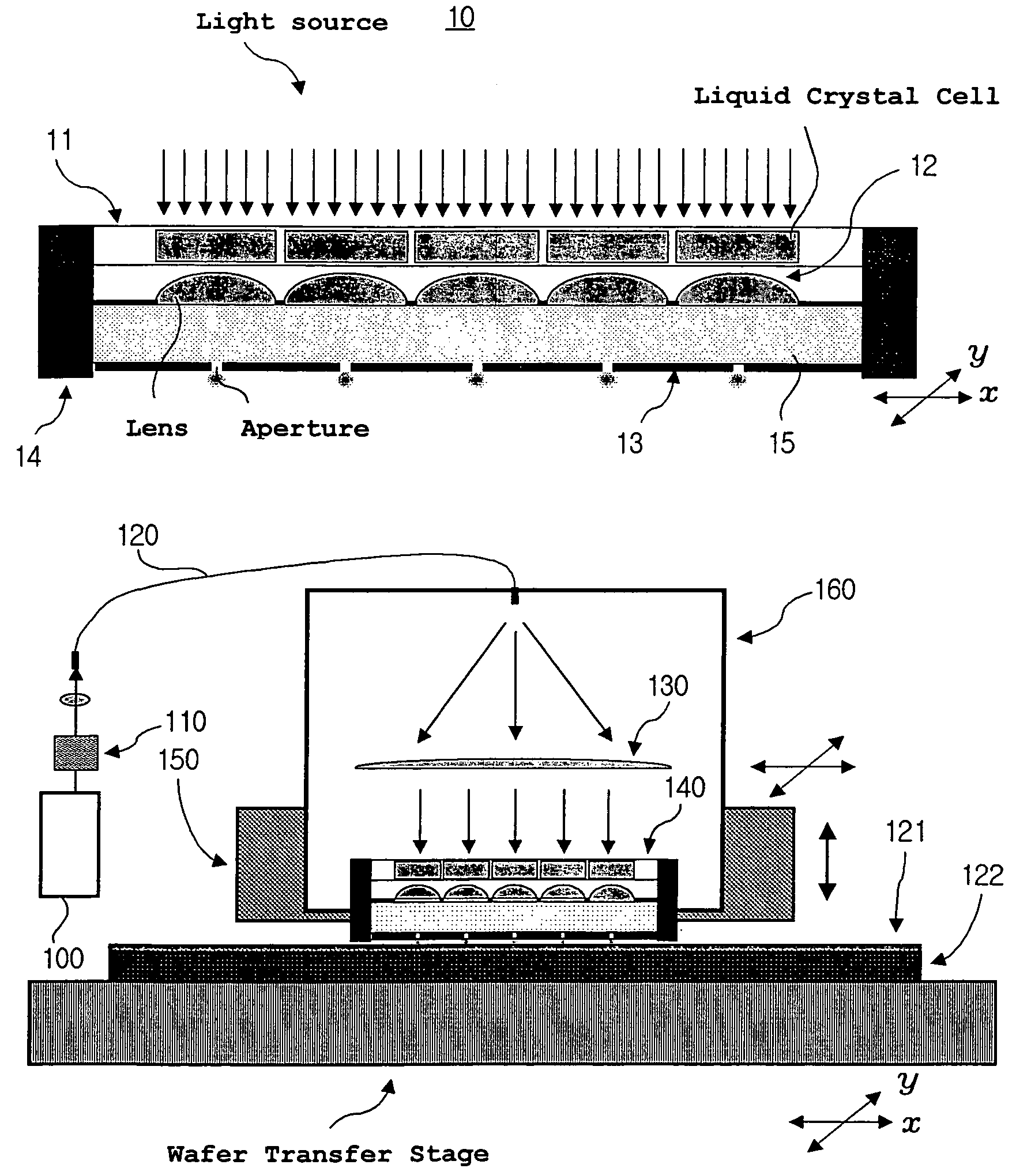
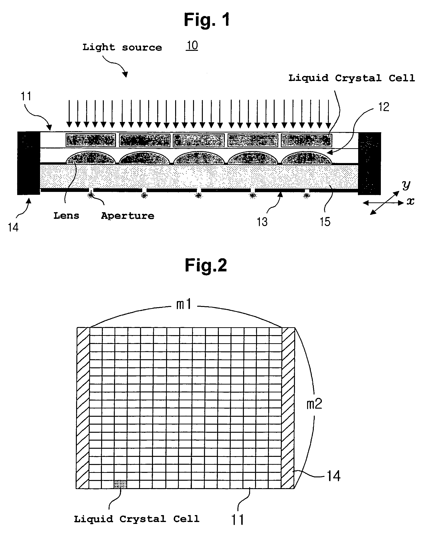
[0025]FIG. 1 is a schematic cross sectional view of a two-dimensional light-modulating fine aperture array apparatus according to the present invention. FIG. 2 is a plan view of a liquid crystal light-modulating unit according to an embodiment of the present invention.

[0026]As shown in FIG. 1, the two-dimensional light-modulating fine aperture array apparatus 10 according to the first embodiment of the present invention comprises a liquid crystal light-modulating unit 11, a microlens array 12, a metal optical waveguide aperture array 13, a distance adjusting unit 14, and a substrate 15.

[0027]The liquid crystal light-modulating unit 11 has a function of adjusting an amount of incident light by using a plurality of liquid crystal cells. As shown in FIG. 2, the (m1×m2) liquid crystal cells are disposed in a two-dimensional array, where m1 and m2 are the numbers of liquid crystal cells in the x and y directions, respectively.

[0028]The liquid crystal light-modulating unit 11 is designed ...

second embodiment

[0050]According to the present invention, since the microlenses having a large numerical aperture NA and the substrate having a high index of refraction are combined, it is possible to greatly reduce the size of a light flux at a focal point as can be explained by Equation 2.

BRIEF DESCRIPTION OF THE DRAWINGS

[0051]The above and other objects, advantages and features of the present invention will become apparent from the following description of preferred embodiments given in conjunction with the accompanying drawings, in which:

[0052]FIG. 1 is a schematic cross sectional view of a two-dimensional light-modulating fine aperture array apparatus according to a first embodiment of the present invention;

[0053]FIG. 2 is a plan view of a liquid crystal light-modulating unit according to an embodiment of the present invention;

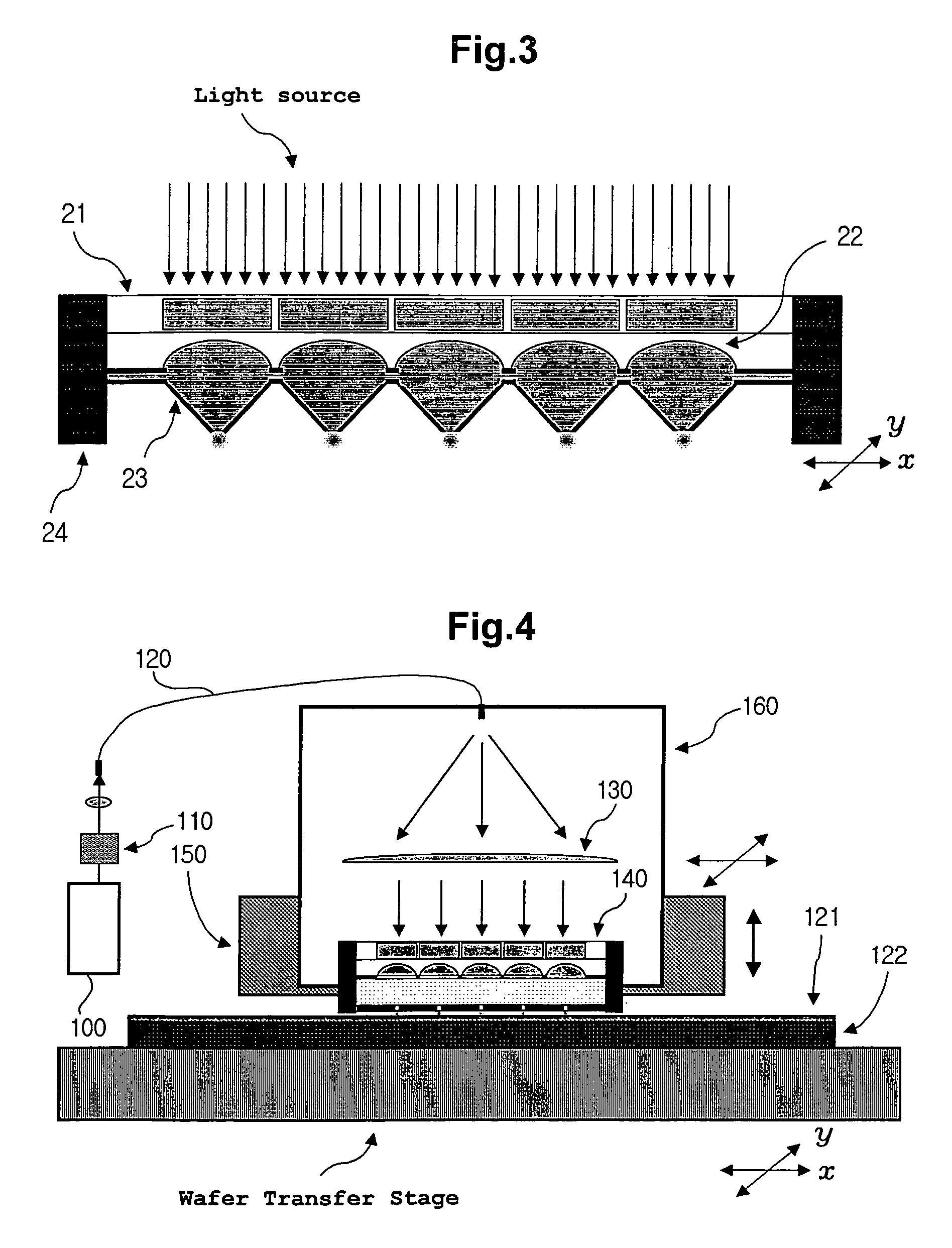
[0054]FIG. 3 is a schematic cross sectional view of a two-dimensional light-modulating fine aperture array apparatus according to a second embodiment of the present inve...


PUM

PropertyMeasurementUnit
wavelengthaaaaaaaaaa
sizeaaaaaaaaaa

Abstract

A two-dimensional light-modulating fine aperture array apparatus includes a spatial light-modulating unit for adjusting quantity of incident light by using a plurality of light amount adjusting cells (liquid crystal cells or micromirrors) arrayed in matrix form, a two-dimensional microlens array having microlenses which focus light beams passing through the light quantity adjusting cells, and a highly efficient two-dimensional fine aperture array. The light is emitted through the fine apertures by connecting the two-dimensional light-modulating fine aperture array apparatus with a light source unit. A scanning unit moves in the x and y directions to perform a scanning process on a surface of a recording medium by using the light emitted from the apertures.

Description

[0001]This application is a continuation-in-part application of pending international application number PCT / KR03 / 01387, filed Jul. 14, 2003, of which the entire disclosure of the pending, prior application is hereby incorporated by reference.TECHNICAL FIELD[0002]The present invention relates to a lithography technique, and more particularly, to a two-dimensional light-modulating fine aperture array apparatus which uses incident light for recording a fine pattern and a high speed fine pattern recording system capable of forming a fine pattern such as a nano pattern on a semiconductor device at a high recording speed by using the two-dimensional light-modulating fine aperture array apparatus.BACKGROUND ART[0003]In general, a lithography technique used to manufacture a semiconductor device includes a masking process and an exposure process. That is, the lithography technique includes steps for preparing a photomask on which a pattern is recorded by using a high precision optical syste...

Claims


Application Information

Patent Timeline
Patent Type & Authority Patents(United States)
IPC IPC(8): G03B27/42G03B27/54G03F7/20H01L21/027
CPCG03F7/70291G03F7/70275H01L21/027B82Y40/00
Inventor HAHN, JAE WON
Owner YONSEI UNIVERSITY
Why Eureka
Try Eureka