Light emitting apparatus and method of fabricating the same
Inactive Publication Date: 2008-07-22
SEMICON ENERGY LAB CO LTD
View PDF63 Cites 90 Cited by
Summary
Abstract
Description
Claims
Application Information
AI Technical Summary
This helps you quickly interpret patents by identifying the three key elements:
Problems solved by technology
Method used
Benefits of technology
Benefits of technology
[0012]Hence, it is an object of the invention to provide a method of selectively forming a high molecular species material layer which is simpler than using an ink jet method in a light emitting apparatus of an active matrix type using a high molecular species organic compound. Further, it is an object thereof to simply form a structure in which the organic compound layer is not formed at a connection portion of a wiring connected to an outside power source by enabling to selectively form the high molecular species material layer.
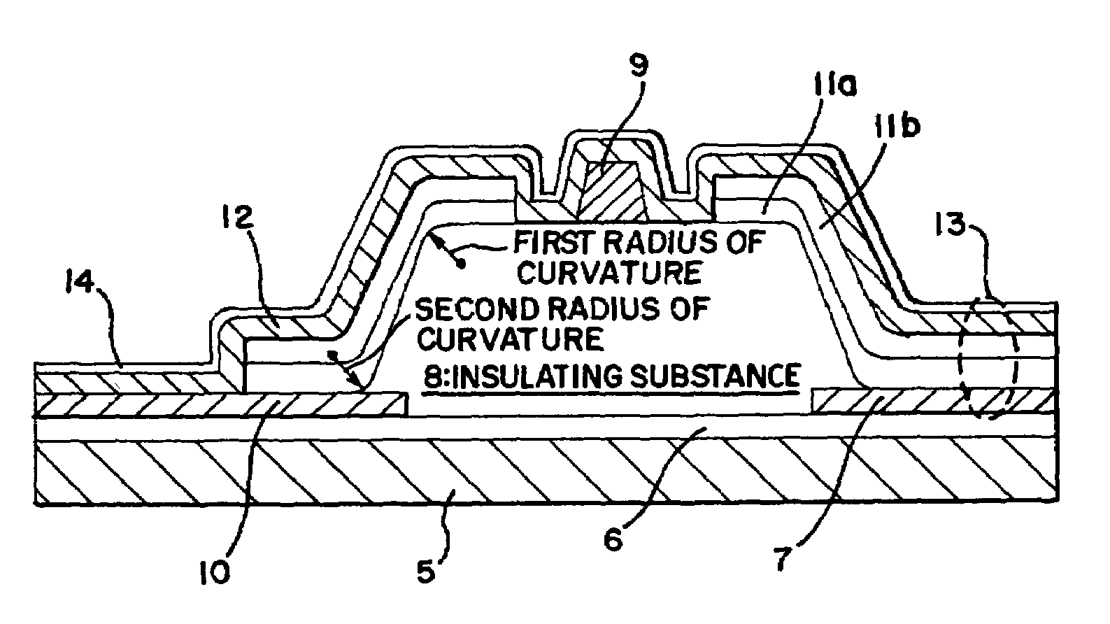
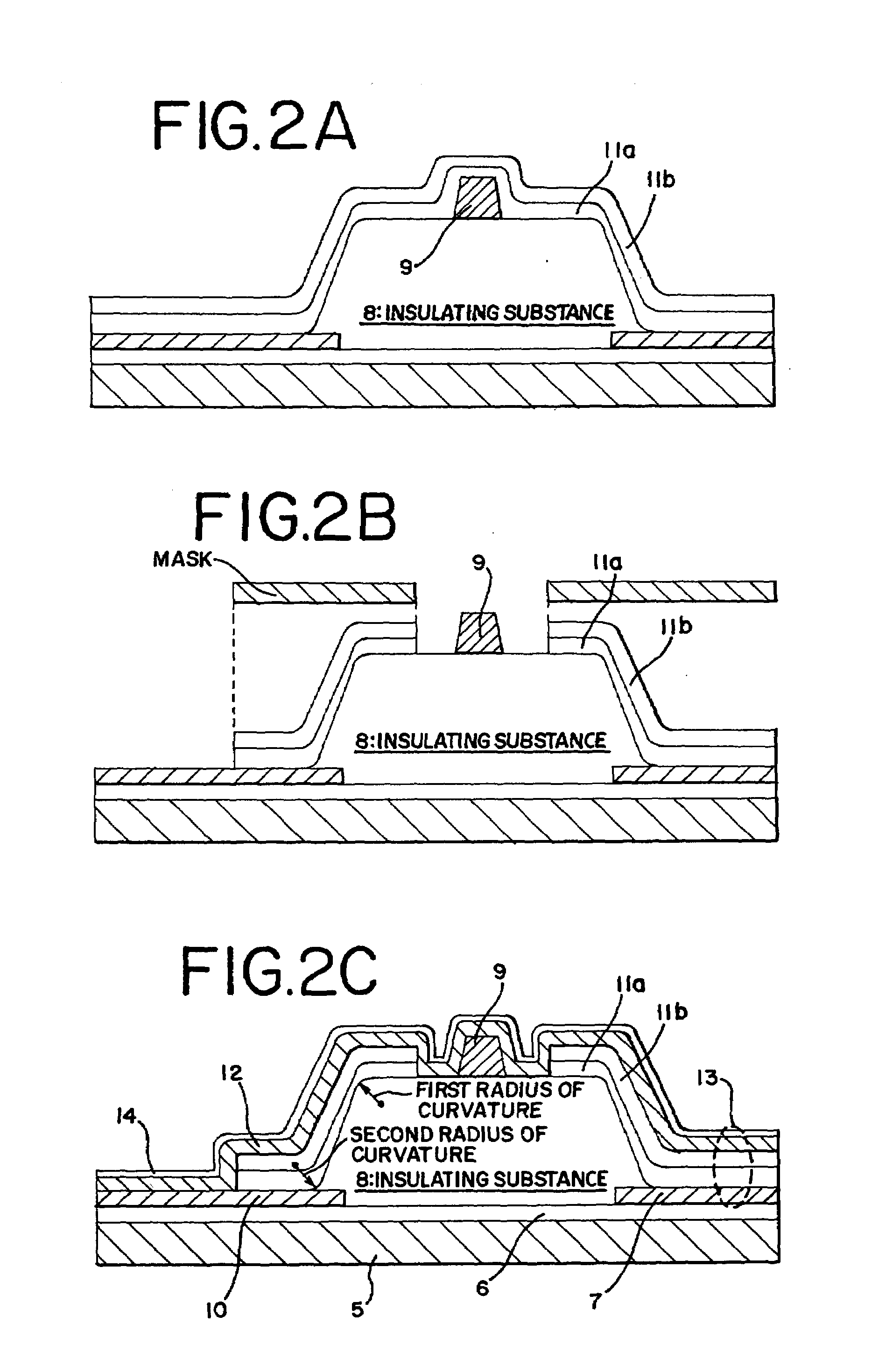
[0039]Further, the invention devises a shape of an insulating substance (referred to as bank, partition wall, barrier, embarkment or the like) provided between respective pixels to eliminate a failure in coverage in forming a high molecular organic compound film by a coating method.
Problems solved by technology
Further, according to a light emitting apparatus, there poses a problem that outside scenery is imaged on an observing face (face directed to a side of an observer) by reflecting incident outside light (light outside of the light emitting apparatus) by a rear face of a cathode (face on a side in contact with a luminescent layer) at a pixel which does not emit light.
Further, in order to avoid the problem, it is devised that a circularly polarized light film is pasted on an observing face of the light emitting apparatus to thereby prevent outside scenery from being imaged on the observing face, however, the circularly polarized light film is very expensive and therefore, there poses a problem of an increase in the fabrication cost.
Method used
Image
Click on the blue label to locate the original text in one second.
Reading with bidirectional positioning of images and text.
Examples
example 1
[0137]According to the example, FIG. 7 shows an example of a fabricating apparatus of a multi-chamber system fully automating fabrication up to an upper electrode.
[0138]In FIG. 7, notations 100a through 100k, 100m through 100w designate gates, notation 101 designates a input chamber, notation 119 designates an output chamber, notations 102, 104a, 108, 114, 118 designate transport chambers, notations 105, 107, 111 designate delivery chambers, notations 106R, 106B, 106G, 106H, 106E, 109, 110, 112, 113 designate film forming chambers, notation 103 designates a pretreatment chamber, notation 117 designates a sealed substrate load chamber, notation 115 designates a dispenser chamber, notation 116 designates a seal chamber, notations 120a, 120b designate cassette chambers, notation 121 designates tray mount stage, notation 122 designates an etching chamber by plasma.
[0139]First, an aqueous solution of poly(ethylenedioxythiophene) / poly(stylene sulfonic acid) (PEDOT / PSS) operated as a hole ...
example 2
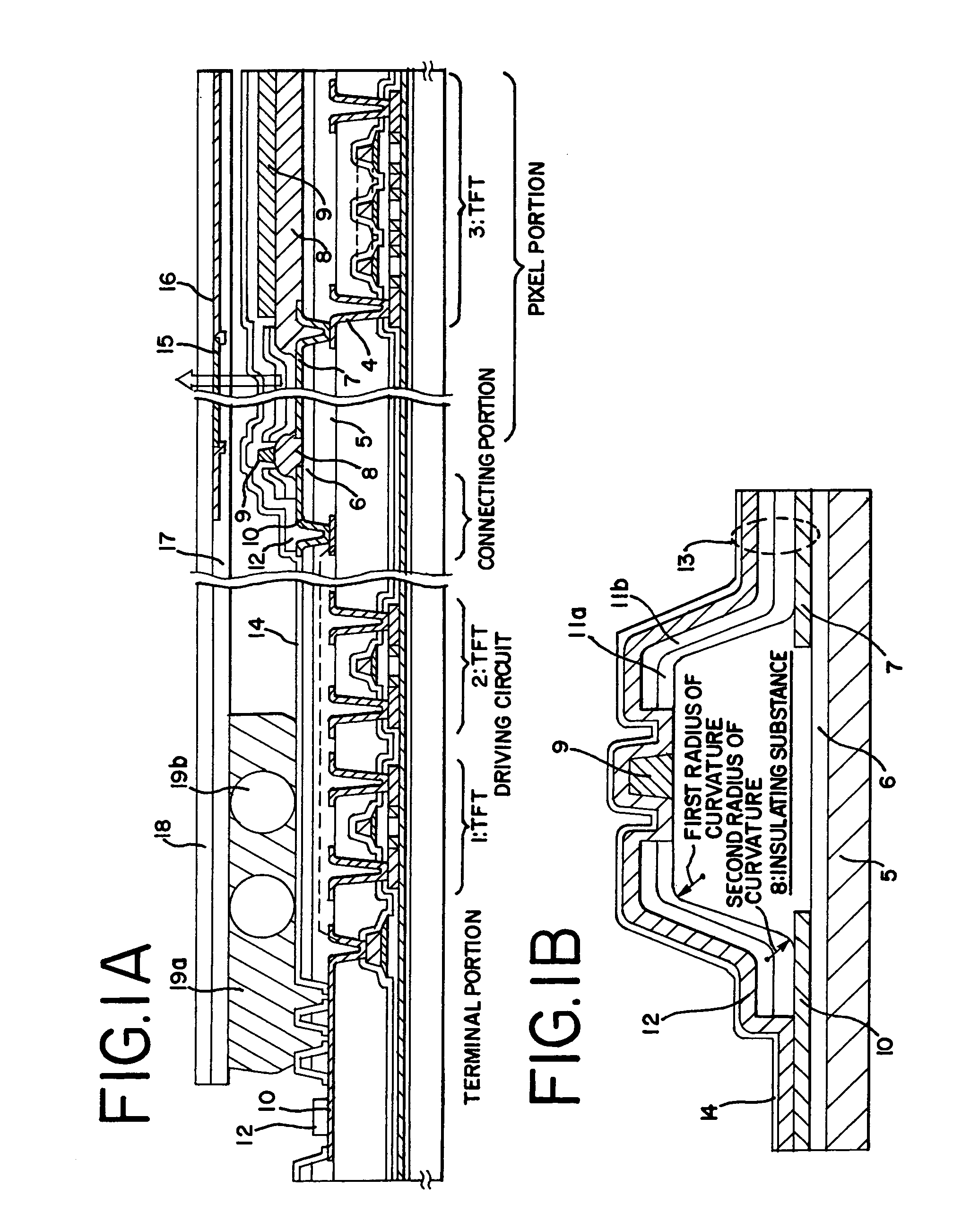
[0173]According to the example, an example of fabricating a structure in which light emitted from an EL element transmits through an element substrate and emitted to enter eyes of an observer will be shown below. Further, in this case, the observer can recognize an image from the side of the element substrate.
[0174]Further, a pixel structure arranged with three TFTs at a single pixel will be explained. Further, FIGS. 9A and 9B show an example of a detailed top view of a pixel.
[0175]A constitution shown by FIGS. 9A and 9B is provided with an erasing transistor 606 in the case of carrying out SES driving, a gate electrode and a second gate signal line 603 for inputting a signal for erasing are connected. A source electrode and-current supply line 604 are connected, and a drain electrode and a drain electrode of a switching TFT 656 and a gate electrode of driving TFT 607 are connected.
[0176]In the case of a three transistor type, two TFTs of the switching TFT 605 and erasing TFT 606 ar...
example 3
[0194]By carrying out the invention, all of electronic apparatus integrated with a module having an organic luminescent element (active matrix type EL module) are completed.
[0195]As such electronic apparatus, a video camera, a digital camera, a head mount display (goggle type display), a car navigation apparatus, a projector, a car stereo, a personal computer, a portable information terminal (mobile computer, portable telephone or electronic book) and the like are pointed out. FIGS. 12A, 12B, 12C, 12D, 12E and 12F and FIGS. 13A, 13B and 13C show examples of these.
[0196]FIG. 12A is a personal computer which includes a main body 2001, an image input portion 2002, a display portion 2003 and a keyboard 2004.
[0197]FIG. 12B is a video camera which includes a main body 2101, a display portion 2102, a voice input portion 2103, an operation switch 2104, a battery 2105, an image receiving portion 2106.
[0198]FIG. 12C is a mobile computer which includes a main body 2201, a camera portion 2202, ...
PUM
Property
Measurement
Unit
Length
aaaaa
aaaaa
Length
aaaaa
aaaaa
Radius
aaaaa
aaaaa
Abstract
Although an ink jet method known as a method of selectively forming a film of a high molecular species organic compound, can coat to divide an organic compound for emitting three kinds (R, G, B) of light in one step, film forming accuracy is poor, it is difficult to control the method and therefore, uniformity is not achieved and the constitution is liable to disperse. In contrast thereto, according to the invention, a film comprising a high molecular species material is formed over an entire face of a lower electrode connected to a thin film transistor by a coating method and thereafter, the film comprising the high molecular species material is etched by etching by plasma to thereby enable to selectively form a high molecular species material layer. Further, the organic compound layer is constituted by a material for carrying out luminescence of white color or luminescence of single color and combined with a color changing layer or a coloring layer to thereby realize full color formation.
Description
BACKGROUND OF THE INVENTION[0001]1. Field of the Invention[0002]The present invention relates to a light emitting apparatus using a luminescent element emitting fluorescence or phosphorescence by applying an electric field to an element having a film including an organic compound (hereinafter, described as “organic compound layer”) between a pair of electrodes and a method of fabricating the light emitting apparatus. Further, a light emitting apparatus in the specification includes an image display device, a light emitting device or a light source (including illuminating device). Further, a light emitting apparatus includes all of a module of a light emitting apparatus attached with a connector, for example, FPC (Flexible Printed Circuit) or TAB (Tape Automated Bonding) tape or TCP (Tape Carrier Package), a module provided with a printed circuit board at a front end of TAB tape or TCP and a module in which a luminescent element is directly mounted with IC (Integrated Circuit) by COG...
Claims
Application Information
Patent Timeline
Application Date:The date an application was filed.
Publication Date:The date a patent or application was officially published.
First Publication Date:The earliest publication date of a patent with the same application number.
Issue Date:Publication date of the patent grant document.
PCT Entry Date:The Entry date of PCT National Phase.
Estimated Expiry Date:The statutory expiry date of a patent right according to the Patent Law, and it is the longest term of protection that the patent right can achieve without the termination of the patent right due to other reasons(Term extension factor has been taken into account ).
Invalid Date:Actual expiry date is based on effective date or publication date of legal transaction data of invalid patent.

