Semiconductor memory device, page buffer resource assigning method and circuit therefor, computer system and mobile electronic device

a memory device and semiconductor technology, applied in memory systems, transistors, instruments, etc., can solve the problems of difficult to reduce the thickness of the gate insulating film, and difficult to realize the reduction in the thickness of the insulating film, so as to achieve the effect of reducing the size of the devi

Inactive Publication Date: 2008-07-29
SHARP KK
View PDF27 Cites 61 Cited by
  • Summary
  • Abstract
  • Description
  • Claims
  • Application Information

AI Technical Summary

Benefits of technology

[0008]The present invention has an objective to provide a semiconductor me...

Problems solved by technology

However, such a flash memory has the following problems: it is functionally necessary that the insulating film 907 is placed to isolate the floating gate 902 from the word line 903; and it is difficult to reduce the thickness of the gate ins...

Method used


Image

  • Semiconductor memory device, page buffer resource assigning method and circuit therefor, computer system and mobile electronic device
  • Semiconductor memory device, page buffer resource assigning method and circuit therefor, computer system and mobile electronic device
  • Semiconductor memory device, page buffer resource assigning method and circuit therefor, computer system and mobile electronic device

Examples


embodiment 1

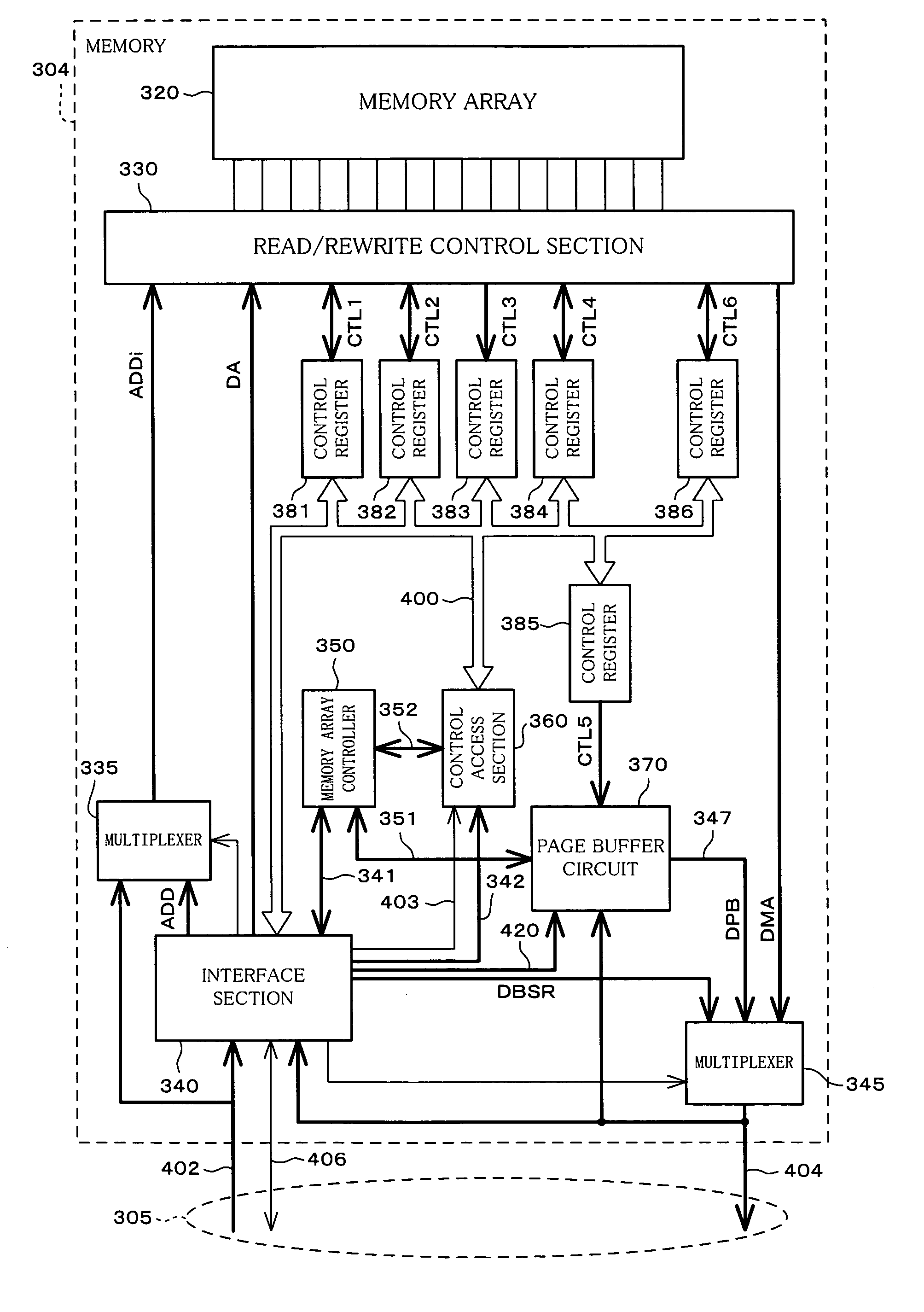
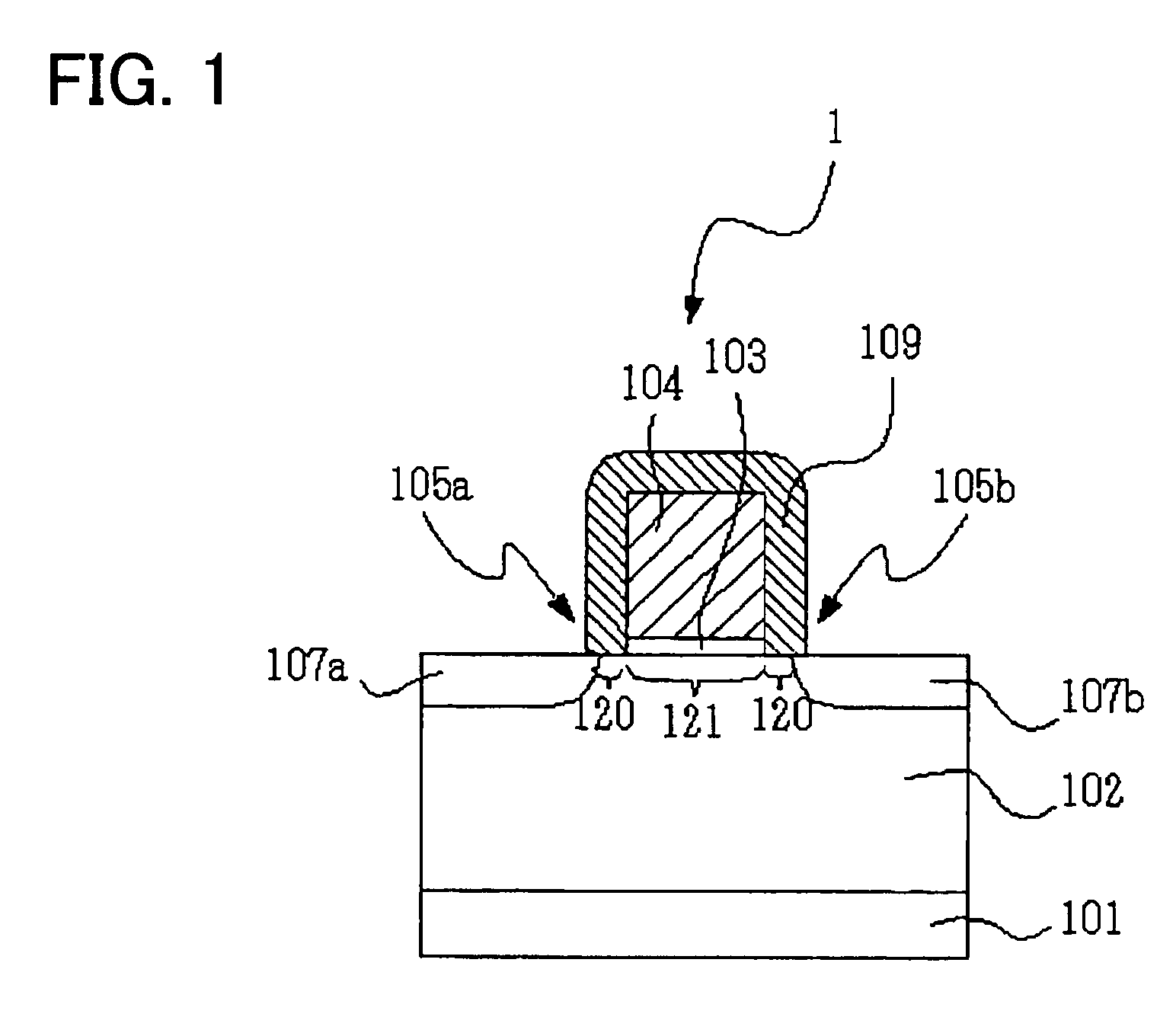
[0085]A semiconductor storage device of the present embodiment includes a memory element 1 as shown in FIG. 1.

[0086]The memory element 1 is arranged such that a gate electrode 104 is formed via a gate insulating film 103 on a P-type well region 102 which is formed on the surface of a semiconductor substrate 101. On the upper surface and side surfaces of the gate electrode 104, arranged is a silicon nitride film 109 which is a charge holding film, holding charges at a trap level. The portions of the silicon nitride film 109 on the both side walls serve as memory functional sections 105a and 105b where charges are actually held. Here, the memory functional section indicates a section where charges are actually accumulated by rewriting operation in a memory functioning member or a charge holding film. In the P-type well region 102 on the opposite sides of the gate electrode 104, formed are N-type diffusion regions 107a and 107b which function as source region or drain region. The diffu...

embodiment 2

[0105]A memory element in a semiconductor storage device of the present embodiment, as shown in FIG. 8, has substantially the same arrangement as that of the memory element 1 in FIG. 1, except for the arrangement in which each memory functioning members 261 and 262 is constituted by a region where charges are held (this region is a region where charges are accumulated and may be a film having a function of holding charges) and a region where charges are less prone to escaping (this region may be a film having a function of making charges less prone to escaping).

[0106]In terms of improvement in holding property of memory, the memory functioning members preferably include an insulating film and a charge holding film capable of holding charges. In the present embodiment, a silicon nitride film 242 having a level of trapping charges is used as a charge holding film, and silicon oxide films 241 and 243 capable of preventing the dissipation of charges accumulated in the charge holding fil...

embodiment 3

[0118]As shown in FIG. 13, a memory functioning member 262 in the semiconductor storage device of the present embodiment includes a silicon nitride film 242, which is a charge holding film, with substantially uniform film thickness, having a region 281 which is arranged substantially parallel to the surface of the gate insulating film 214 and a region 282 which is arranged substantially parallel to the side surface of the gate electrode 217.

[0119]When a positive voltage is applied to a gate electrode 217, an electric flux line 283, as indicated by arrow, in a memory functioning member 262 passes through the silicon nitride film 242 twice (the region 282 and the region 281). Note that, when a negative voltage is applied to the gate electrode 217, an electric flux line reverses its direction. Here, the silicon nitride film 242 has a relative permittivity of approximately 6, and the silicon oxide films 241 and 243 have a relative permittivity of approximately 4. This arrangement of the...


PUM


Abstract

A semiconductor memory device includes a page buffer circuit and an arrangement of memory elements each including: a gate electrode provided on a semiconductor layer with an intervening gate insulating film; a channel region provided beneath the gate electrode; a diffusion area provided on both sides of the channel region, having an opposite polarity to the channel region; and a memory functioning member provided on both sides of the gate electrodes, having a function of storing electric charge. The page buffer circuit provides a common resource shared between a memory array controller and a user. The page buffer circuit has two planes containing random access memory arrays. The page buffer circuit also includes a mode control section to facilitate access to the planes over a main bus in user mode and access to the planes by the memory array controller in memory control mode.

Description

[0001]This Nonprovisional application claims priority under 35 U.S.C. § 119(a) on Patent Application No. 2003-142750 filed in Japan on May 20, 2003, the entire contents of which are hereby incorporated by reference.FIELD OF THE INVENTION[0002]The invention relates to integrated semiconductor memory devices and in particular to page buffer resource assignment for semiconductor memory devices.BACKGROUND OF THE INVENTION[0003]Conventionally, a flash memory has been used as a nonvolatile memory.[0004]In this flash memory, as shown in FIG. 30, a memory cell is constituted such that a semiconductor substrate 901 includes thereon, via a gate insulating film, a floating gate 902, an insulating film 907, and a word line (control gate) 903 in this order, and a source line 904 and a bit line 905 are formed on both sides of the floating gate 902. Around the memory cell, an element separation region 906 is formed (for example, Japanese Laid-Open Patent Application No. 304277 / 1993 (Tokukaihei 5-3...

Claims


Application Information

Patent Timeline
IPC IPC(8): G11C16/00G06F12/00G11C7/10G11C16/02G11C16/04G11C16/10H01L21/8247H01L27/10H01L27/115H01L29/788H01L29/792
CPCG11C7/10G11C16/10G11C7/1039G11C2207/2245
Inventor YAOI, YOSHIFUMIIWASE, YASUAKIIWATA, HIROSHISHIBATA, AKIHIDEMORIKAWA, YOSHINAONAWAKI, MASARU
Owner SHARP KK
Why Eureka
Try Eureka