Measuring method and its apparatus

a measurement method and apparatus technology, applied in the field of scanning electron microscope, can solve the problems of inability inability to perform the measurement method with high accuracy in the case of a small number of models, and inability to achieve the ability to obtain a dimension corresponding to the cross-sectional shape of the pattern

Active Publication Date: 2008-08-05
HITACHI HIGH-TECH CORP
View PDF11 Cites 15 Cited by
  • Summary
  • Abstract
  • Description
  • Claims
  • Application Information

AI Technical Summary

Benefits of technology

[0010]It is another object of this invention to provide a measuring method and its apparatus that brings about fewer models to be prepared beforehand by enabling accurate measurement with fewer models at the time of dimension measurement when applying a model that the apparatus stores beforehand to an image profile of the pattern to be measured.
[0014]According to various aspects of the invention, the scanning electron microscope is able to control a pattern bottom dimension which affects, for example, characteristics of a transistor as a result of enabling the measuring of a pattern dimension at a desired position on a cross-sectional shape of a pattern using an image profile obtained from a scanning electron microscope image of the pattern.
[0015]According to various aspects of the invention, it becomes possible to employ fewer models to be prepared beforehand because accurate measurement is enabled with fewer models at the time of dimension measurement when applying a model that the apparatus stores beforehand to an image profile of the pattern to be measured. Further, by thus performing dimension measurement when applying a model to an image profile of the pattern to be measured, it becomes possible to perform relatively accurate measurement on a low S / N image as well.

Problems solved by technology

However, in these methods, since a measuring position is determined from only the obtained image profile information, there is no clear correlation between a measuring position detected from the image profile and a measuring position in the cross-sectional shape of the pattern.
However, there is a disadvantage have in that it is costly and time-consuming to perform these methods.
Further, in the method for measuring pattern dimensions by verifying the image profile of a pattern to be measured against a library of image profiles of various cross-sectional shapes that have been created beforehand with an electron beam simulation, as disclosed in non-patent document 1, the ability to obtain a dimension corresponding to the cross-sectional shape of the pattern has not been achieved at this time.
Further, measuring dimensions with the method disclosed in non-patent document 1 is based on the assumption that models of various dimensions and shapes have been prepared in large quantities, whereas there is a problem in that dimension measurement cannot be performed with high accuracy in the case of a small number of models.

Method used


Image

  • Measuring method and its apparatus
  • Measuring method and its apparatus
  • Measuring method and its apparatus

Examples


embodiment 1

[0036]The present invention aims to measure a dimension of a fine pattern using an image obtained by picking up an image of the fine pattern with a scanning electron microscope.

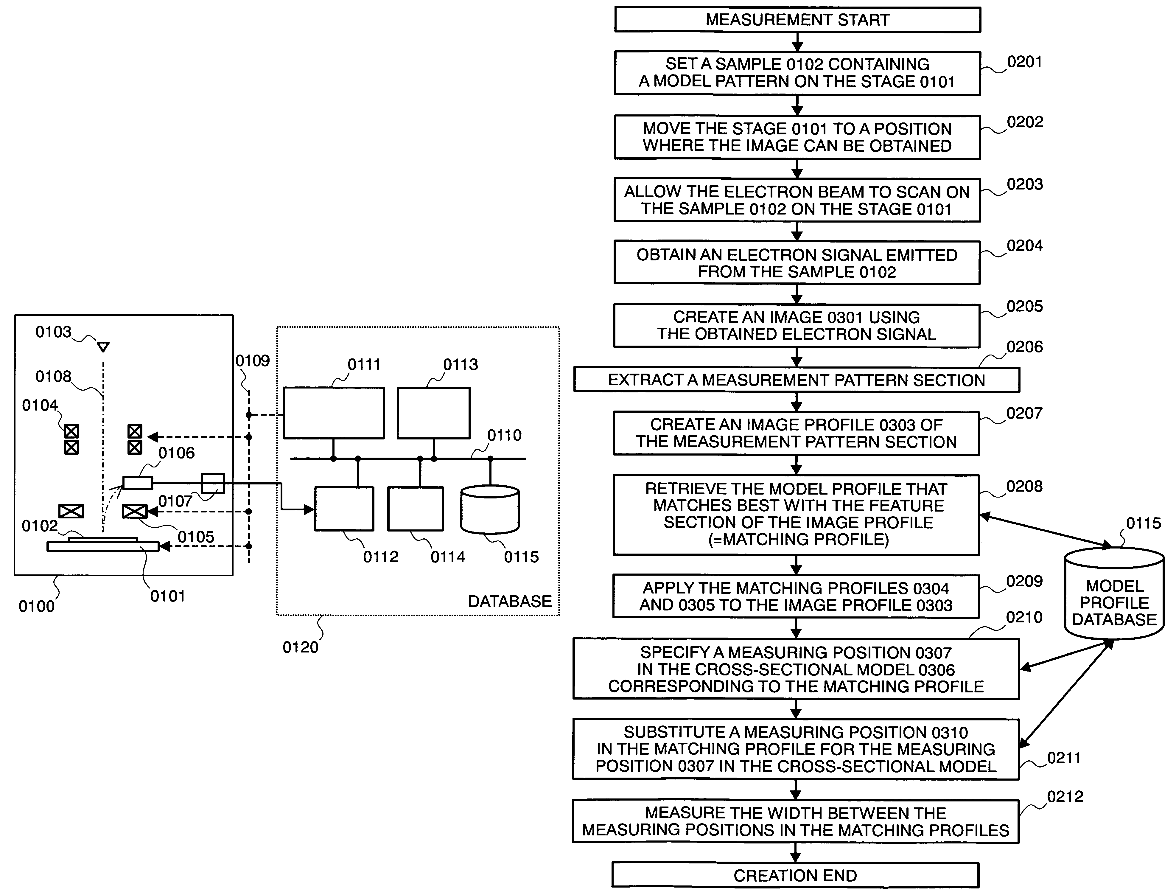
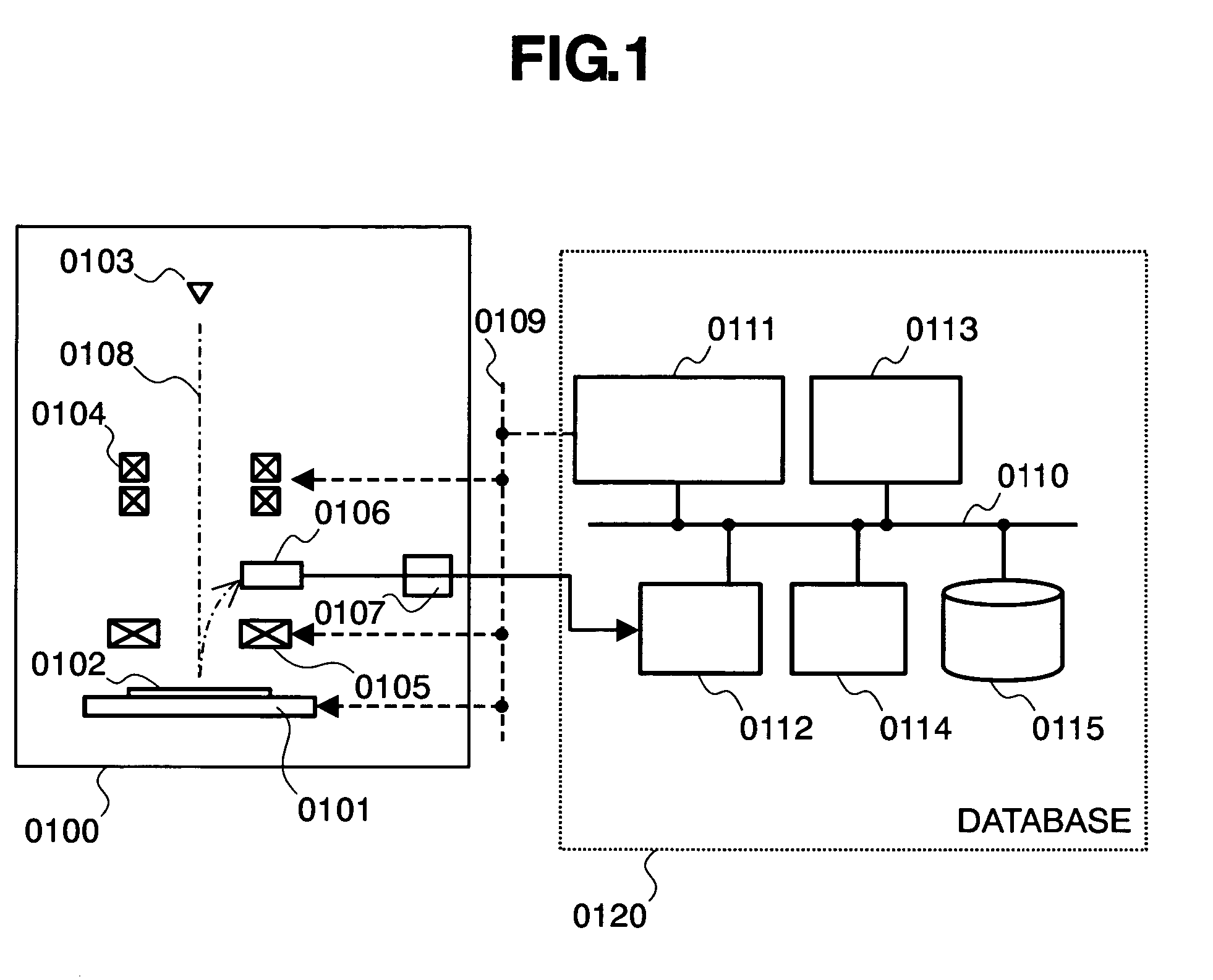
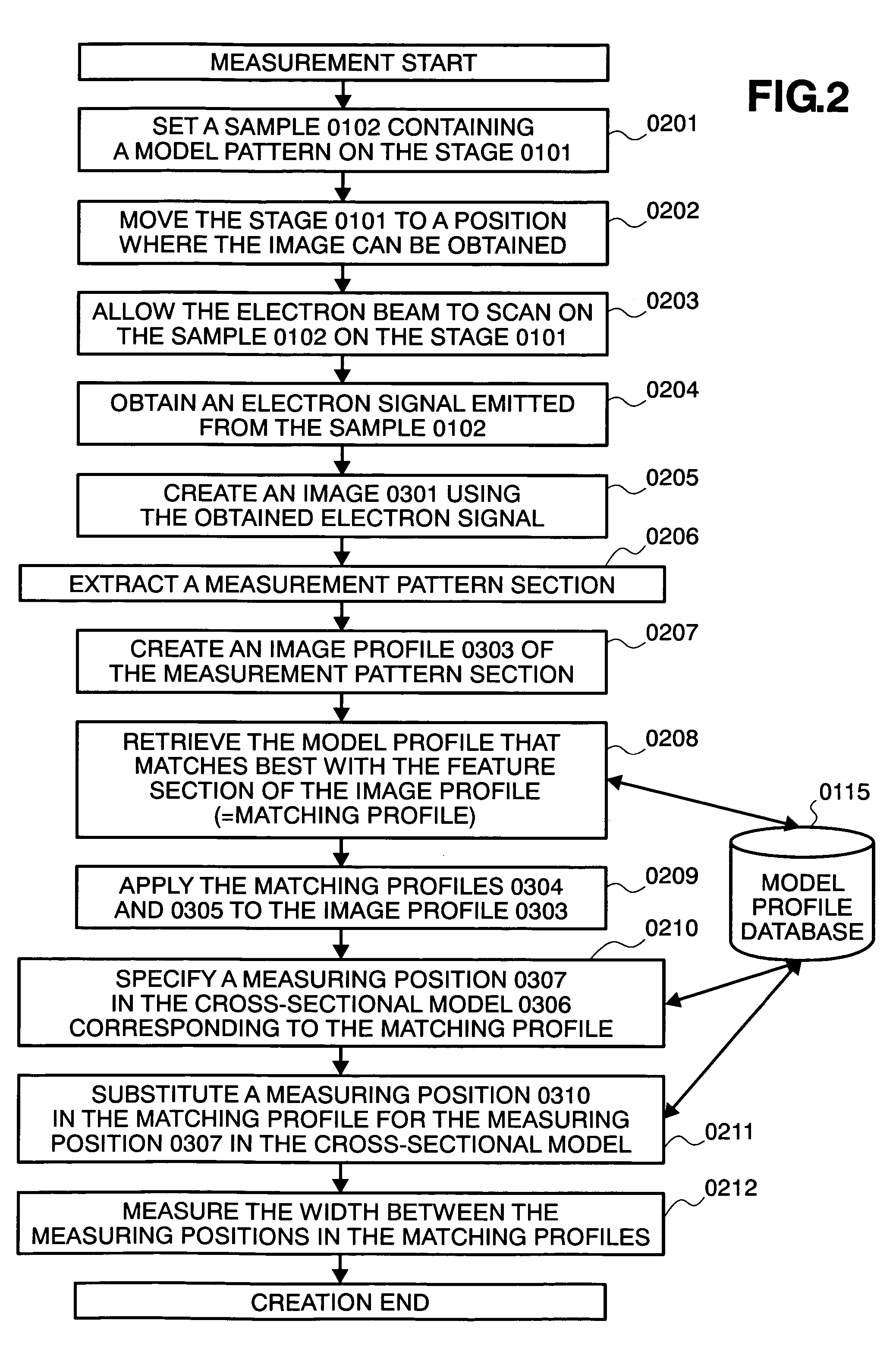
[0037]FIG. 1 shows the structure of a scanning electron microscope apparatus according to the present invention. This apparatus is divided broadly into two parts, which consist of an electron optics system 0100 for obtaining electron beam images and an information processing system 0120 for measuring an object pattern by processing the electron beam images. The electron optics system 0100 mainly includes a stage 0101 on which a sample 0102 is mounted, an emission source 0103 which emits an electron beam 0108, a deflector lens 0104 which deflects the electron beam 0108, an objective lens 0105 which is controlled to pick up an image at the in-focus position, a secondary electron detector 0106 which has the function of converting the secondary electrons coming from the sample into an electric signal, and an A / D ...

embodiment 2

[0073]This embodiment is directed to facilitation of the process of creating the database 0115 shown in FIG. 4. In this embodiment, a dimension measurement is performed with a model profile and a cross-sectional model (which are stored in the database) created using a shape that varies in stages, such as a pattern on an FEM (Focus Expose Matrix) wafer created by changing the exposure value and focus in stages in accordance with a position on the wafer. By employing a model profile and a cross-sectional model whose shapes are predicted to vary in stages makes it possible, instead of obtaining the dimension of a pattern under measurement by determining one model profile that matches with the image profile of the pattern, to obtain the dimension of the pattern under measurement by interpolation processing using one or more selected cross-sectional models and model profiles that match relatively well with the image profile and resemble it in shape. Therefore, even in the case of a small...


PUM

PropertyMeasurementUnit
widthaaaaaaaaaa
incident angleaaaaaaaaaa
dimensionaaaaaaaaaa

Abstract

A method for measuring a dimension of a pattern formed on a sample using a secondary electron image obtained by picking up an image of the sample using a scanning electron microscope includes: obtaining a secondary electron image of a sample by picking up an image of the sample using a scanning electron microscope; creating, using the secondary electron image, an image profile of a pattern whose dimension is to be measured, within the obtained secondary electron image; retrieving a model profile that matches best with the created image profile from a plurality of model profiles prestored that are obtained from respective secondary electron images of a plurality of patterns, the cross sections of the plurality of patterns being of known shapes and dimensions and being different in shape; and obtaining a dimension of the pattern using information of the retrieved model profile.

Description

BACKGROUND OF THE INVENTION[0001]The present invention relates in general to an electron microscope of the types used for measuring a dimension of a fine pattern formed on a semiconductor substrate, and, more particularly, the invention relates to a scanning electron microscope having the function of calculating measurement data associated with a dimension measuring position in a cross section of a pattern.[0002]In semiconductor wafer manufacturing processes, finer design of multilayer thin-film patterns formed on a wafer has been advancing rapidly, and process monitoring to monitor whether or not the patterns are formed as designed is becoming increasingly important. According to the 2002 edition of the ITRS (International Technology Roadmap for Semiconductors), which shows a roadmap for finer patterns of semiconductors, it is anticipated that the wiring pattern width of a transistor gate, where the finest pattern on a semiconductor wafer is formed, will become approximate 25 nm or...

Claims


Application Information

Patent Timeline
Patent Type & Authority Patents(United States)
IPC IPC(8): G03F7/20G03F7/40
CPCG01N23/225
Inventor OOSAKI, MAYUKAKAWADA, HIROKINAKAGAKI, RYOSHISHIDO, CHIE
Owner HITACHI HIGH-TECH CORP
Why Eureka
Try Eureka