
Systems, circuits and methods for extending the detection range of an inspection system by avoiding detector saturation

a technology of inspection system and detection range, applied in the direction of electron multiplier details, optical radiation measurement, instruments, etc., can solve the problems of single detector being saturated, device to fail, and inability to inspect different types of wafers, etc., to achieve the effect of enhancing defect detection

Active Publication Date: 2008-08-19
KLA TENCOR TECH CORP
View PDF28 Cites 8 Cited by
  • Summary
  • Abstract
  • Description
  • Claims
  • Application Information

AI Technical Summary

Benefits of technology

"The patent describes a system and method for inspecting a specimen by detecting light scattered from it using a photomultiplier tube (PMT) detector. The system includes an illumination subsystem for directing light to the specimen and a detection subsystem for generating a first signal and a second signal in response to the detected light. The detection subsystem uses a dynode current of the PMT detector until it reaches a predetermined threshold, at which point it switches to using the second signal. The system can also include a collector for collecting the light scattered from the specimen and a load for converting the anode current into another voltage to produce the second signal. The technical effect of this invention is to enhance defect detection by addressing anode saturation as a limiting factor of the measurement detection range of the PMT detector."

Problems solved by technology

For instance, detecting defects of decreasing size has become increasingly necessary, since even relatively small defects may cause unwanted aberrations in the semiconductor device, and in some cases, may cause the device to fail.
In addition, most inspection tools are designed to inspect either unpatterned or patterned semiconductor wafers, but not both.
Since the tools are optimized for inspecting a particular type of wafer, they are generally not capable of inspecting different types of wafers for a number of reasons.
In some cases, the single detector may become saturated, and as a result, may not yield signals that can be analyzed for defect detection.
Even if the single detector does not become saturated, the light scattered from patterns or other features on the wafer cannot be separated from other scattered light thereby hindering, if not preventing, defect detection based on the other scattered light.
However, the detectors used in patterned wafer inspection tools may also become saturated, especially when imaging with a dark-field system.
It is often difficult, especially with detection systems operating at high data rates, to collect meaningful signals from both the very dark and the very bright areas of the substrate being inspected without “on-the-fly” adjustment.
Most optical inspection tools are limited in either detection range, detection sensitivity, or both.
For example, inspection tools employing high-gain detectors to obtain higher detection range may be incapable of detecting smaller (i.e., low light) signals.
In other words, although lower gain detectors may be capable of detecting smaller signals, they may become saturated when larger signals are received.
Other factors tend to limit the detection range, in addition to detector gain.
For example, further limitations may be imposed by the amplification circuitry or the fast analog-to-digital converters used to convert the scattered output signals into a format suitable for signal processing.
Although this approach may provide improved visibility of small-signal defects in the dark-field image, it does nothing to extend the overall detection range of the inspection system.
In addition, the “on-the-fly” gain modulation disclosed by Wolf causes the PMT to be operated in a highly non-linear way, thus requiring complex (and expensive) drive electronics and sophisticated calibrations to compensate for the non-linear and transient effects.
Though Almogy is able to extend the detection range, Almogy does so by requiring multiple detectors with additional optics and electronic circuitry, all of which consume additional space, increase complexity, and incur higher cost.

Method used


Image

  • Systems, circuits and methods for extending the detection range of an inspection system by avoiding detector saturation
  • Systems, circuits and methods for extending the detection range of an inspection system by avoiding detector saturation
  • Systems, circuits and methods for extending the detection range of an inspection system by avoiding detector saturation

Examples


Embodiment Construction

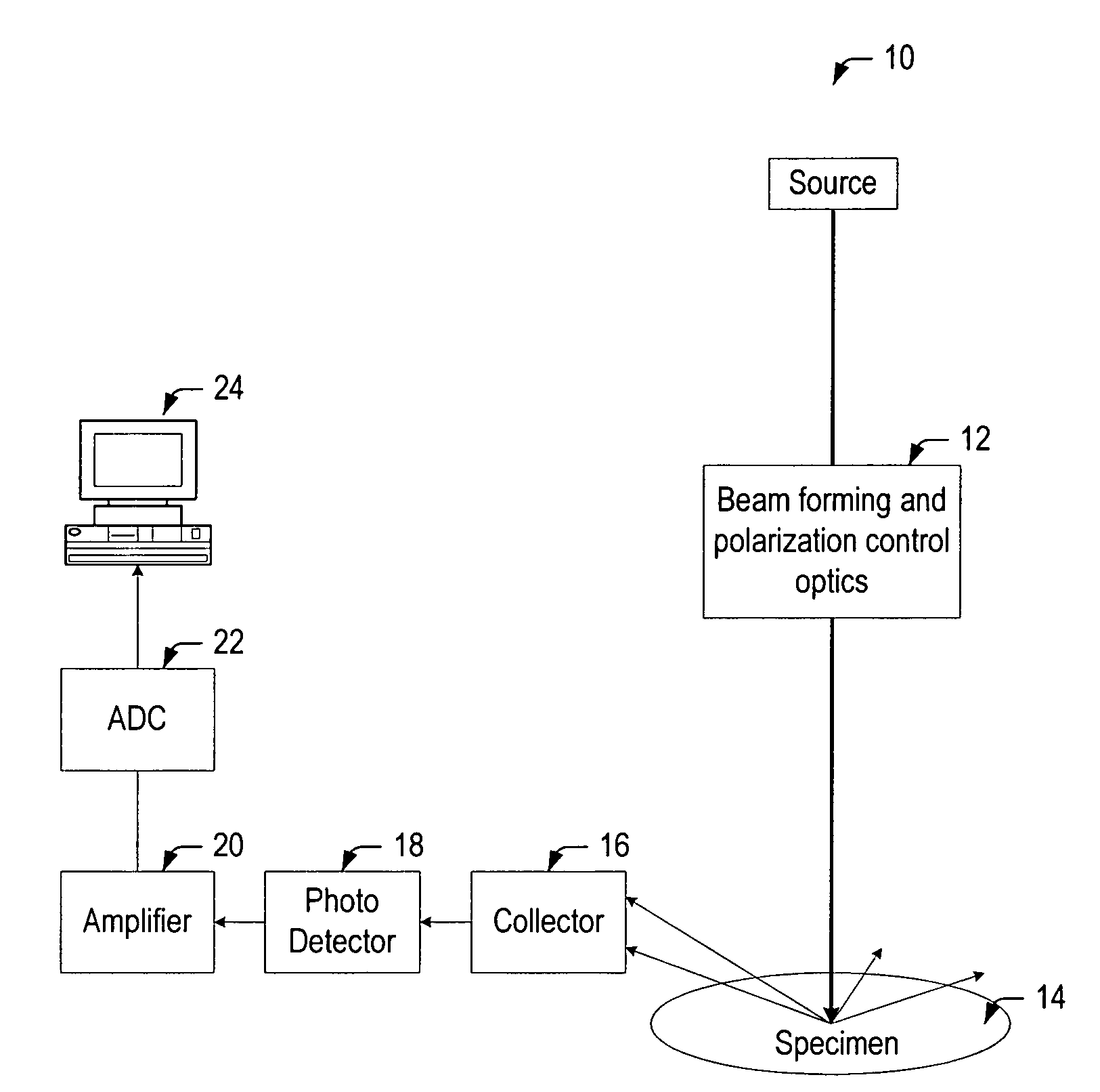
[0038]The methods and systems described herein enhance defect detection by addressing various limiting factors of measurement detection range including, but not limited to, detector saturation, amplifier saturation and the fixed bit range of analog-to-digital converters (ADC). Unlike some currently used inspection methods, the inspection system described herein is able to extend the measurement detection range while maintaining signal linearity and stability, and without employing additional detectors, optics and electronic components, all of which undesirably increase space consumption, complexity and cost of the inspection system.

[0039]Various embodiments are described herein for an optical inspection system or tool that may be used for inspecting a specimen. The term “specimen” is used herein to refer to a wafer, a reticle, or any other sample that may be inspected for defects, features, or other information (e.g., an amount of haze or film properties) known in the art.

[0040]As u...


PUM

PropertyMeasurementUnit
wavelength rangeaaaaaaaaaa

Abstract

Inspection systems, circuits and methods are provided to enhance defect detection by addressing anode saturation as a limiting factor of the measurement detection range of a photomultiplier tube (PMT) detector. In accordance with one embodiment of the invention, a method for inspecting a specimen includes directing light to the specimen and detecting light scattered from the specimen. The step of detecting may include monitoring an anode current of the PMT detector, and detecting features, defects or light scattering properties of the specimen using the anode current until the anode current reaches a predetermined threshold. Thereafter, the method may use a dynode current of the PMT for detecting the features, defects or light scattering properties of the specimen.

Description

BACKGROUND OF THE INVENTION[0001]1. Field of the Invention[0002]The present invention generally relates to circuits, systems and methods for extending a measurement detection range of an inspection system used for inspecting a specimen. More specifically, the present invention relates to circuits, systems and methods for extending the measurement detection range of an inspection system by addressing the anode saturation of a photomultiplier tube (PMT) as a limiting factor of the measurement detection range.[0003]2. Description of the Related Art[0004]Fabricating semiconductor devices, such as logic, memory and other integrated circuit devices, typically includes processing a specimen such as a semiconductor wafer using a number of semiconductor fabrication processes to form various features and multiple levels of the semiconductor devices. For example, lithography is a semiconductor fabrication process that typically involves transferring a pattern to a resist arranged on a semicond...

Claims


Application Information

Patent Timeline
Patent Type & Authority Patents(United States)
IPC IPC(8): G01N21/00
CPCG01N21/47H01J43/30G01N21/9501G01N21/21G01N21/95607
Inventor WOLTERS, CHRISTIAN H.ROMANOVSKY, ANATOLYSLOBODOV, ALEXANDER
Owner KLA TENCOR TECH CORP
Learn More